DC/DC switching power converters (Adell et al., 2002,2003) produce DC output voltages from different DC input sources. In addition, DC/DC converters are commonly used to provide noise isolation, and power bus regulations.A switching power converter uses energy storage elements such as inductors, or capacitors to transfer energy from the input to the output at periodic intervals. This energy transfer results in a change in the DC output voltage relative to the input voltage, producing electrical isolation between the input and the output. DC/DC switching power converters are being used for spacecraft power systems, motor drives,computers, telecommunications, and military and industrial applications.
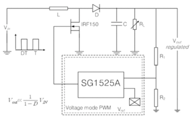
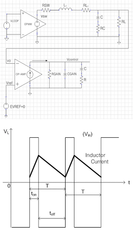
The converters can be used in regenerative braking of DC motors to return energy back into the supply, resulting in energy savings for the systems containing frequent stops. The ideal DC/DC converter (Lho et al., 2007) exhibits 100% efficiency, but efficiency is 70 to 95% in practice. Pulse width modulation (PWM) is applied to control and regulate the total output voltage. There are three kinds of DC/DC converters exist: a) The boost converter as a step-up converter is used for cases in which a higher output voltage than input is required; b) a buck converter as a step-down converter is used for cases in which a lower output voltage than input is required; and c) a buck-boost converter, which reduces or increases the voltage ratio with a unit gain for a duty ratio of 50%. This paper focuses on the boost converter(Adell et al., 2002) and the buck converter (Adell et al.,2003) by using of switched-mode power supply (SMPS).Typically, PWM circuits operate on either a current mode or a voltage mode. This study focuses on the voltage mode in pulse-width modulation. Figure 1 shows a schematic of the boost converter composed of linear circuits as well as a comparator, an operational amplifier, and voltage reference.The integrated PWM under evaluation is the SG1525AJ-ND for IC PWM regulating switching pulse 16-DIP. The use of different feedback capacitors produces a strong effect on the transient response of the hybrid integrated circuit.
The greater the capacitance, and the greater the load resistance, the smaller the ripple effect becomes, which is measured at the output of the PWM and the boost converter.The output voltage of the ideal boost converter is given by

where D is the variable duty cycle.
The basic voltage-mode PWM buck converter is composed of the same components as the boost converter. However, the locations of metal-oxide semiconductor field effect transistor(MOSFET), diode, and inductor differ. The output voltage of the ideal buck converter is given by

where the duty cycle D is dynamically adjusted by the feedback circuit to keep a stable DC output voltage.
2. SPICE Model and Specifications
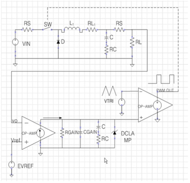
Figures 1 and 2 show a basic voltage-mode PWM boost converter for the simulation program with integrated circuit emphasis (SPICE) model (Cadence Design Systems, 2004).When the MOSFET remains off for a long period of time,the voltage across the capacitor assumes the same value as the input voltage. When the MOSFET is on, the DC input voltage appears across the inductor, and the diode prevents the capacitor from discharging to ground. Thus, the current(Lee et al., 2006) through the inductor increases linearly as the input voltage divided by the inductance rises. When the MOSFET is off during the discharge phase, the voltage(Lee et al., 2006) across the inductor abruptly changes in
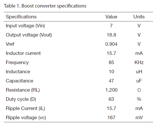
[Table 1.] Boost converter specifications

Boost converter specifications
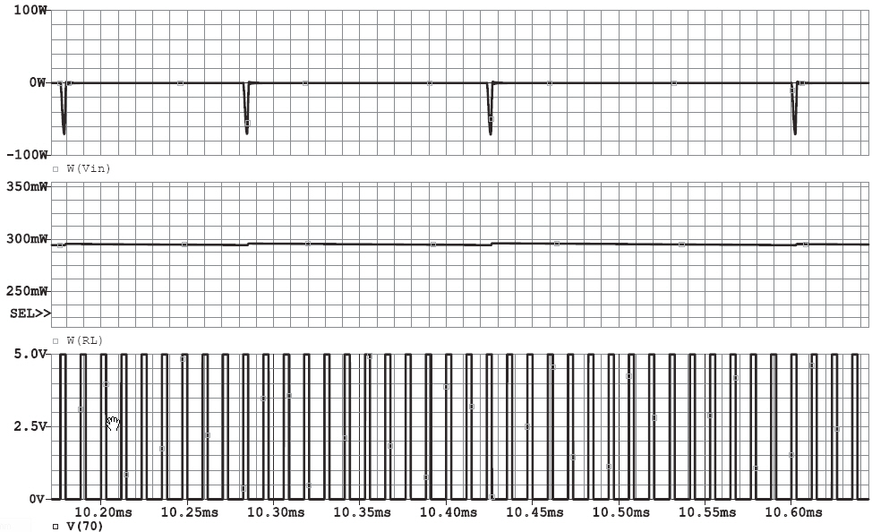
order to maintain current flow. This effect occurs because the inductor current cannot change instantaneously. The feedback circuit follows input voltage by controlling the duty cycle at the gate of the MOSFET (Rho et al., 1997), or by controlling the required output voltage over variations in loading. Figure 3 shows a schematic of the buck converter.The IRF150 MOSFET is replaced by the ideal switch in the buck converter with SMPS as shown in Fig. 4
Table. 1 and 2 show the specifications of the boost converter and the buck converter studied in this work,respectively.
[Table 2.] Buck converter specifications
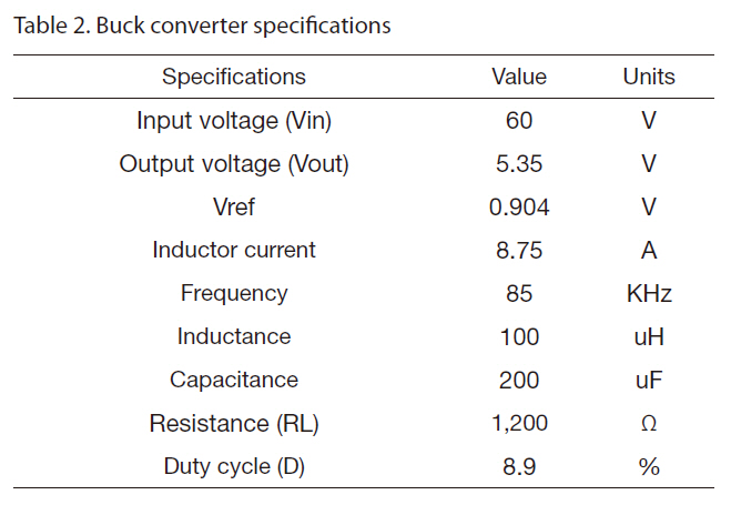
Buck converter specifications
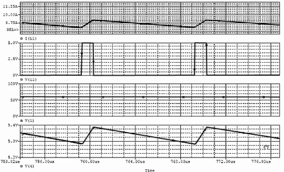
For the analysis, it is assumed that the inductor current is always flowing. The voltage across the inductor is shown in Fig. 5, and the average of this voltage must be zero in order for the average current to remain in steady state.


and for a lossless circuit, the input and output ratio becomes to

The output voltages shown in Figs. 1 and 2 must always be higher than the input voltage in magnitude because the duty ratio of D is between 0 and 1. The slope of current flowing at the inductor is computed as

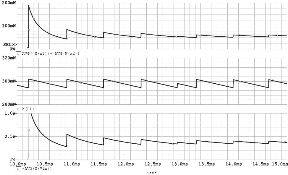
When the MOSFET is on, the slope of inductor current increases linearly until the IRF 150 MOSFET is off. The slope can be written as shown in Eq. (6). When the MOSFET is off subsequently changing into a breakdown voltage (Rho and Kim, 2005) of 150 V, the inductor current and the output voltage decrease with time constant of 0.24. Figure 6 illustrates the input power of W(Vin) consumed across inductor, the output power of W(out), and the pulse at output terminal of comparator. The power dissipated at both the PWM IC and MOSFET, the output power, and the input power during the duration of time between 10.5 to 15 ms under steady state are shown in Fig. 7. The applied resistors of R1 and R2 in Figs. 1 and 2 are 190 KΩ and 10 KΩ, respectively.
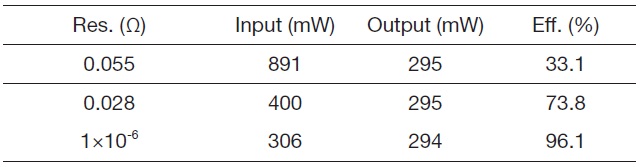
[Table 3.] The efficiency based on load resistance

The efficiency based on load resistance
The total input power is dissipated at both MOSFET and PWM IC. The power consumed in PWM IC is computed as follows.

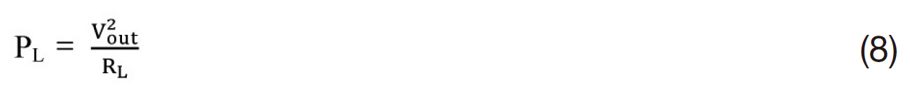
where Ibias in simulation is the current of 14 mA flowing in the SG1525A voltage mode pulse width modulator IC, f is the frequency with a value of 85 Khz, and Qg is the gate charge with a value of 120 nC for turning-on the MOSFET.The power is 24.2 mW. When the specifications in Table 1 is applied to the boost converter, an output power (PL) of 295 mW is obtained by
where Vout converges to 18.8 V.
The maximum on-resistance (Ron), which indicates the static drain-to-source on-state resistance in electrical characteristics at the room temperature of 25℃ of IRF150 MOSFET, is 0.055Ω This leads to a power efficiency of 33.1% after a time lapse of 10.2 ms for the output power in steady state. In order to reduce the on-resistance of the MOSFET,two IRF150 components are arranged in parallel. The input power becomes 400 mW and the output becomes 295 mW.The power efficiency reaches 73.8%. For an the ideal switch,in which MOSFET is replaced by an on-resistance of 1μΩ the input power and the output power become 306 and 294 mW,respectively. Additionally, the power efficiency is reached 96.1%. The dominant factor affecting of the power efficiency is the on-resistance at load. As the on-resistance in MOSFET decreases, producing a higher value in the gate charge, the power factor increases. As the gate charge increases, the power efficiency decreases. An appropriate gate charge value is required for the high power efficiency.
As the value of duty cycle increased from 0.1 to 0.9 by 0.2,the output of Vout increased sharply. The value of D applied to this configuration in Figs. 6 and 7 is 0.25.
In order to determine the values of the current flowing in the inductor and the voltage across the inductor, the wave form of the voltage, as shown in Fig. 4, was applied to the buck converter. In effect, the inductor current decreased with the time constant when the switch was off. The simulations in Fig. 8 satisfy these theories. The output voltage in the buck converter decreased to 5.35 for an applied input voltage of 60 V. The applied duty cycle for the buck converter remained the same as that of the boost converter.
The characteristics of a DC/DC converter containing a PWM module were successfully simulated by SPICE, and satisfy the computed values. The inductor current in the simulation decreased with the time constant, which is met with the theoretical voltage and current waveform shown in Fig. 3. The dominant factor for producing a high power efficiency is the low on-resistance in correlation with an appropriate increased gate charge. The design parameter of a low on-resistance and an appropriate low gate charge should be considered in order to achieve high power efficiency.