Carbon nanotubes (CNTs) have been considered to be an ideal field emitter due to their unique characteristics, such as large aspect ratio with small tip radius of curvature and high chemical stability [1-3]. CNT field emitters have been prepared by mainly two techniques. One is the screenprinting of CNT paste [4,5] and the other is the direct growth of CNTs by chemical vapor deposition [6,7]. The screenprinting is known to be more useful than its counterpart when the field emitter is prepared on the large size substrates, for example, the application of CNTs into large size flat panel display. In addition, the fact that one can use high quality thin multiwall (MW) CNTs synthesized independently is another advantage of this technique since the synthesis of the high quality CNTs on glass substrate by CVD method is not straightforward due to limited growth temperature. For the practical application of CNT paste into the field emission devices, the paste emitter should have long-term emission stability. For this reason, many researchers have been trying to evaluate and improve the emission stability of CNT paste emitters [8-10]. However,most studies were carried out in vacuum chamber of which environment is quite different from that in the practical sealed device. In this study, it was found that the CNT paste emitter in the sealed device is much more stable than that in a vacuum chamber despite the similar pressure of ~1 ×10⁻⁶Torr. For further improvement in the life-time of sealed field emission devices, a couple of approaches (DC plasma treatment and electrical aging) were applied to increase the emission stability of CNT paste.
Thin multiwall carbon nanotubes (t-MWCNTs) with diameters of 3~5 nm were used to prepare photo-sensitive CNT paste. One weight percent of CNTs were mixed with negative-type photo-sensitive resin, organic vehicles, and inorganic powders in a solvent. The paste was screen-printed on indium tin oxide (ITO) coated glass substrate, followed by drying at 65℃ for 20 min. The backside of screen-printed substrate was exposed to ultraviolet (UV) light and then developed by ethyl-cellusolve. The substrate was fired at 450℃ in nitrogen atmosphere, followed by adhesive tape treatment for forming the field emitter with vertically aligned CNTs. Scanning electron microscope (SEM) and transmission electron microscope (TEM) were used to investigate the morphologies of CNT powder and CNT emitters prepared. The stability of CNT emitter was measured at a constant voltage (CV) mode in both vacuum chamber and fully sealed device. The measurements were carried out with a parallel diode configuration connected to pulse-generator. The distance between anode and cathode was 200 ㎛. The emitter was exposed to inert gas (Ne/Xe) plasma in order to get uniform heights of CNT tips. The effect of aging condition on the emission stability was also investigated.
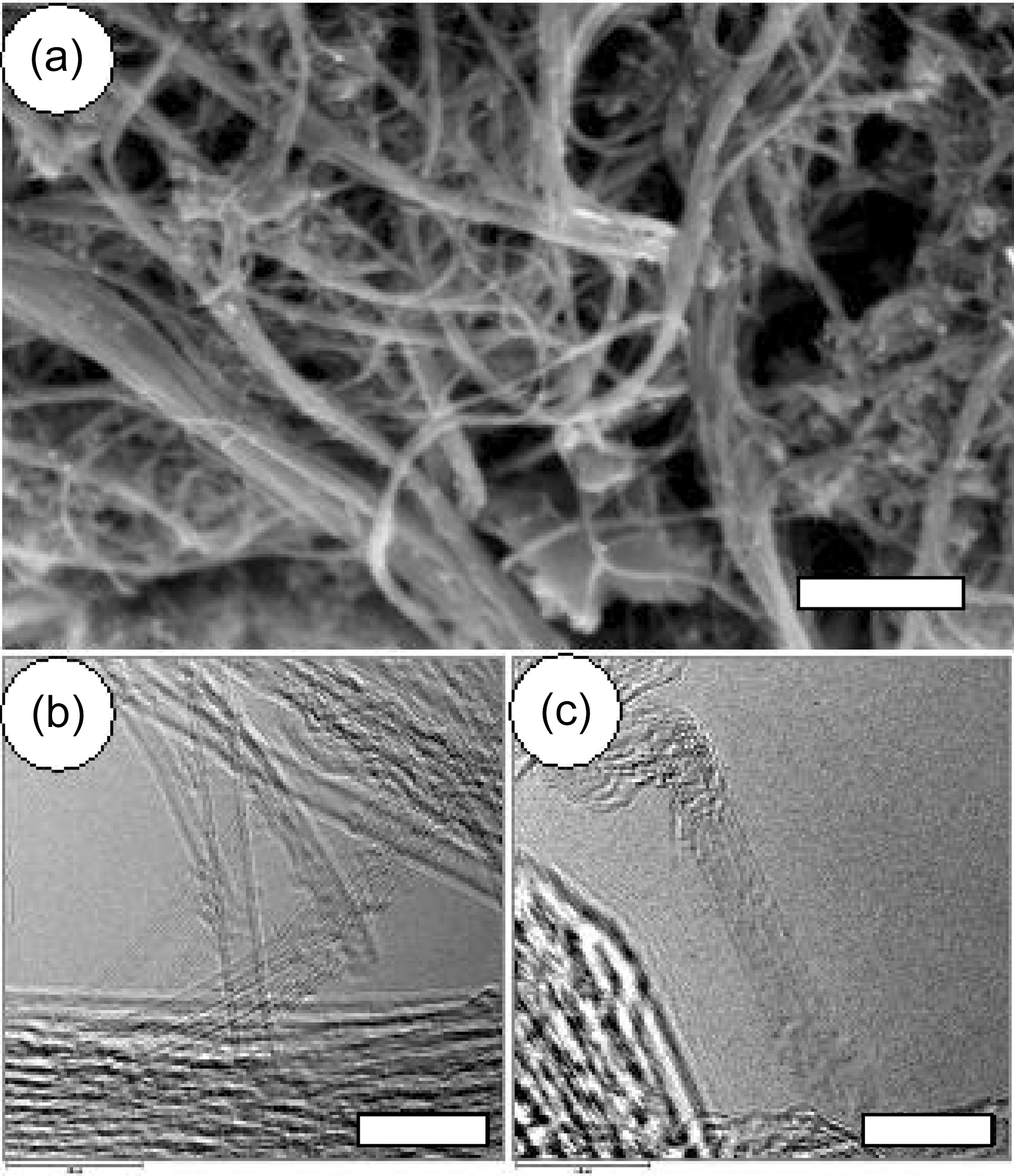
Fig. 1 shows the SEM and TEM images of pristine CNTs used to prepare CNT paste. The SEM image shown in Fig. 1(a) represents the CNTs have very high purity without any noticeable impurities. Thermogravimetric analysis (TGA) showed that the powders are composed of ~98 wt% CNTs and~2 wt% catalyst metal particles. The CNTs were found to have uniform diameters of 3~5 nm with 2~4 graphitic walls,as shown Figs. 1(b) and (c).
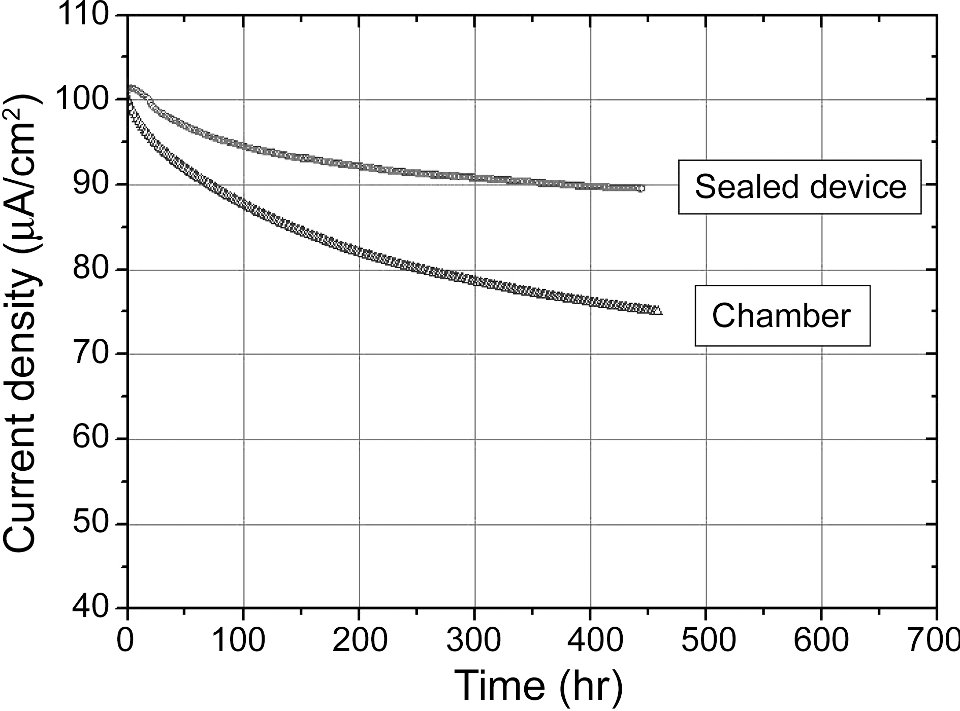
Fig. 2 shows the current density vs. time characteristic of CNT paste emitters measured in vacuum chamber and fully sealed device. The measurements were carried out with an initial current density of 100 μA/cm2 at 0.1% duty ratio, which is similar to the driving condition of practical field emission display. The emitter was prepared by the screen printing of CNT paste with a size of 2 cm×2 cm. The emitter was non-patterned, in other words, whole emitter area (4 cm2) was covered by the CNT paste. Before the measurements, the electrical aging was carried out at 300 μA/cm2 with 0.1% duty ratio for 10 min. This electrical treatment was reported to be helpful for achieving uniform emission by increasing the emission site density [11]. Since higher density of emission site is expected to be beneficial for longer life-time of the field emission devices, the electrical aging is carried out for all samples in this study.Both samples measured in the vacuum chamber and the sealed device show similar current-voltage (I-V) characteristic with turn-on electric fields of ~3 V/㎛. (not shown here) However, it was found from Fig. 2 that the packaging process increased the emission stability drastically. After 400 hrs, the current density measured in the chamber decreases to 75 μA/cm2(25% decrease) while the emitter in the sealed device is still emitting high current density of 90 μA/cm2 (10% decrease). This phenomenon has reproducibly observed in the CNT paste emitters. In order to elucidate the cause of difference, the environment inside vacuum chamber (the type of gases remaining and their partial pressures) was examined by residual gas analyses (RGA) while the chamber was being pumped out by turbomolecular pump. The gases found in the chamber were N2 (~74%), O2 (~19%), CO2 (~5%), and H2 (~1%). The total pressure (~1×10⁻⁶Torr) and corresponding partial pressures of these gases were found to be kept almost constant while the chamber was being pumped out, which implies that the vacuum chamber is not perfectly closed system. In other words, the oxygen gas was continuously supplied into the chamber, inducing the oxidative etching of CNT tips. This is because Joule heating-induced high temperature of the emitting tips burn-out the nanotubes [12,13]. In contrast, the sealed device was almost closed system that prevents the supply of oxygen. The pressure inside the sealed device was measured to be ~1.23×10⁻⁶Torr. The remaining gases and their partial pressures were N2 (5.5×10⁻⁷Torr), CH4 (1.96×10⁻⁷Torr), Ar (1.98×10⁻⁷Torr), C2H6 (1.16×10⁻⁷Torr), H2 (1.06×10⁻⁷Torr), CO2 (5.76×10⁻⁸Torr), and H2O (5.27×10⁻⁹Torr). Since the barium getter loaded in the sealed device could easily adsorb most O2 gas, we could hardly observe O2 gas. Although H2O and CO2 are also believed to cause the oxidative degradation of CNTs during field emission, the amount of those gases are not very large enough to attack CNTs seriously. Hence, it is believed that the oxidation of CNT tips is not severe in sealed device, which might have resulted in the high emission stability of CNT paste. Basically, the emission stability of CNT emitter is dependent on the vacuum level. For example, ultra high
vacuum chamber with a pressure of ~10-9Torr results in very long-term stability of CNT emitters. However, such high vacuum state is not possibly achieved in the practical device. The purpose of the present study is to evaluate the emission stability of CNT emitter in the practical environment. It can be therefore said that the stability measured in the sealed device is more meaningful than that observed in the vacuum chamber.
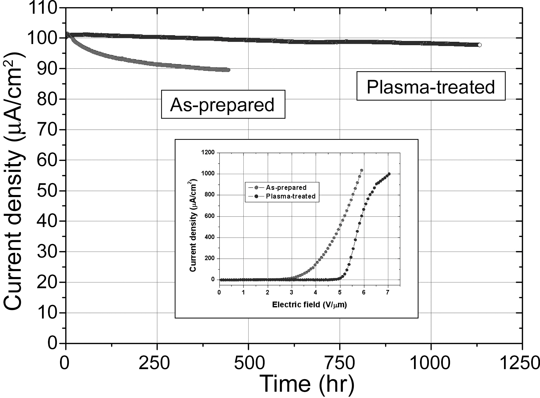
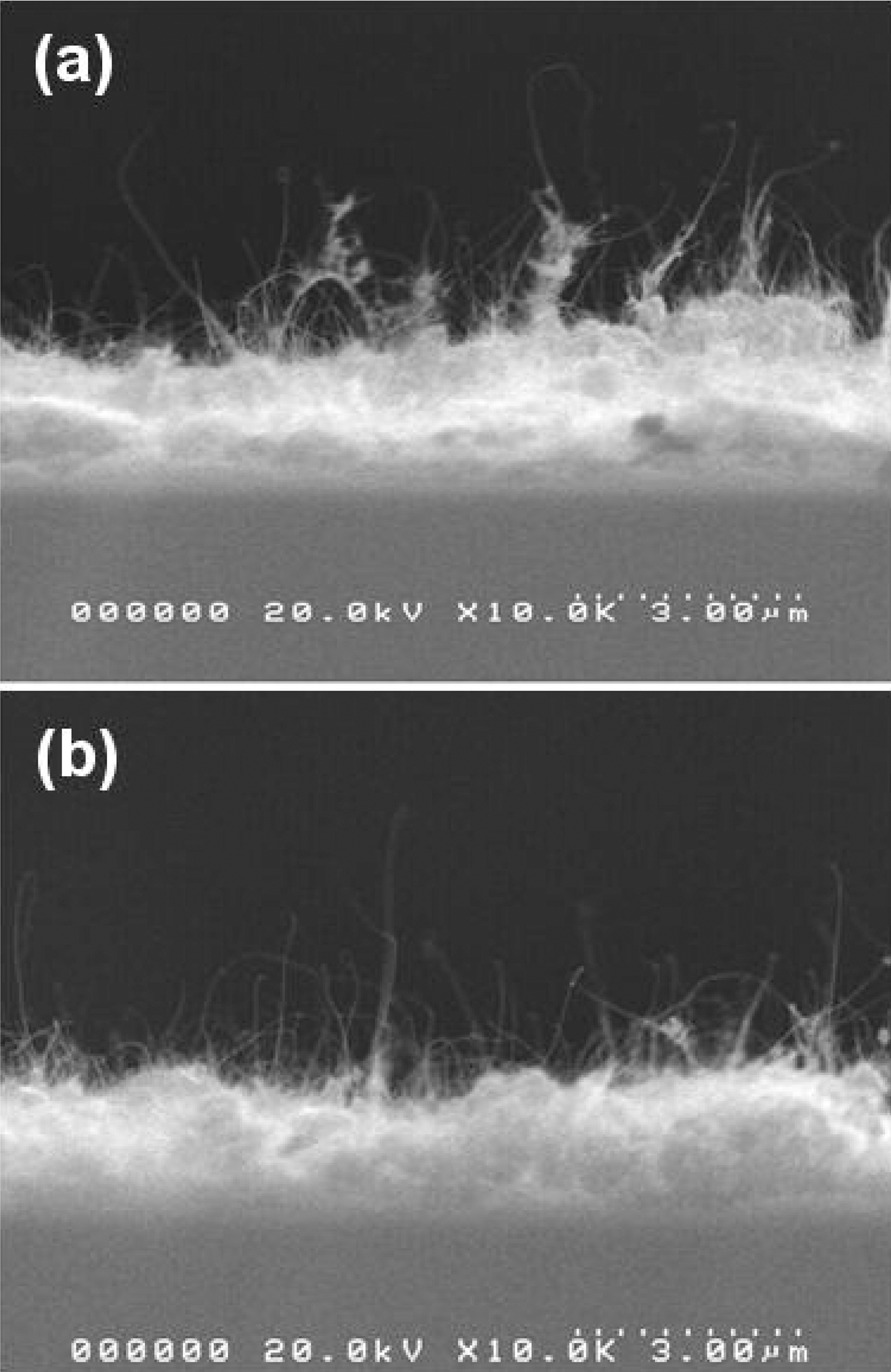
It has been reported that uniform height of emission tips is one of the prerequisites for the high performance of field emitter [14,15]. While CVD-grown vertically aligned CNT emitter has in general uniform heights [16], achieving uniform tip-heights in the CNT paste emitter is not straightforward since the paste underwent physical surface treatment for forming the emitter. In order to overcome this drawback of CNT paste, we treated the paste emitter by DC plasma. The gas mixture of Ne(85%)/Xe(15%) was fed into the vacuum chamber. The plasma was generated by applying 250 V with the distance between CNT emitter and counter electrode of 1 mm. Fig. 3 shows that the plasma treatment changes the surface morphology of the CNT emitter. Long CNTs on the surface of field emitters are selectively removed, resulting in relatively uniform tip heights. Fig. 4 represents the stabilities
of as-prepared and plasma-treated CNT paste emitters formed in the sealed device. Inset in Fig. 4 shows the current-voltage (I-V) curves of two emitters. The plasma treatment increased the turn-of field of CNT emitter from 3 V/㎛ to 5 V/㎛. This is attributed to the elimination of protruded long CNT tips by the plasma treatment, as shown in Fig. 3. The initial current density of 100 μA/cm2 was obtained by applying the electric fields of 3.75 V/mm and 5.3 V/mm to as-produced and plasma-treated emitters, respectively. The as-produced CNT paste emitter shows the decrease of current by 10% during 400 hrs, which is the same data as that shown in Fig. 2. The DC plasma treatment was found to increase the stability markedly. Even after 1,000 hrs, only ~2% decrease in the current density was observed. As was seen in Fig. 3, the uniformity of CNT-tip heights was improved by the plasma treatment. It is therefore believed that the increased stability observed after the plasma treatment is due probably to the uniform heights of CNT tips. The life-time is generally defined as the duration during which the current decreases to the half of its initial value. By extrapolating the current density vs. time curve, the life-time of plasma-treated CNT emitter is expected to be around ~25,000 hrs. Since current decreasing rate is in general getting retarded with time, the life-time is expected to be longer than 25,000 hrs, which is believed to be long enough for applications.
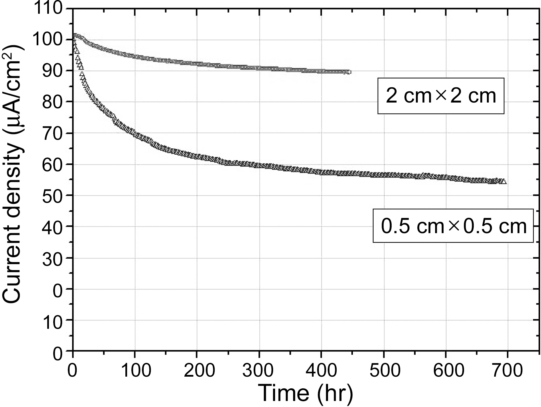
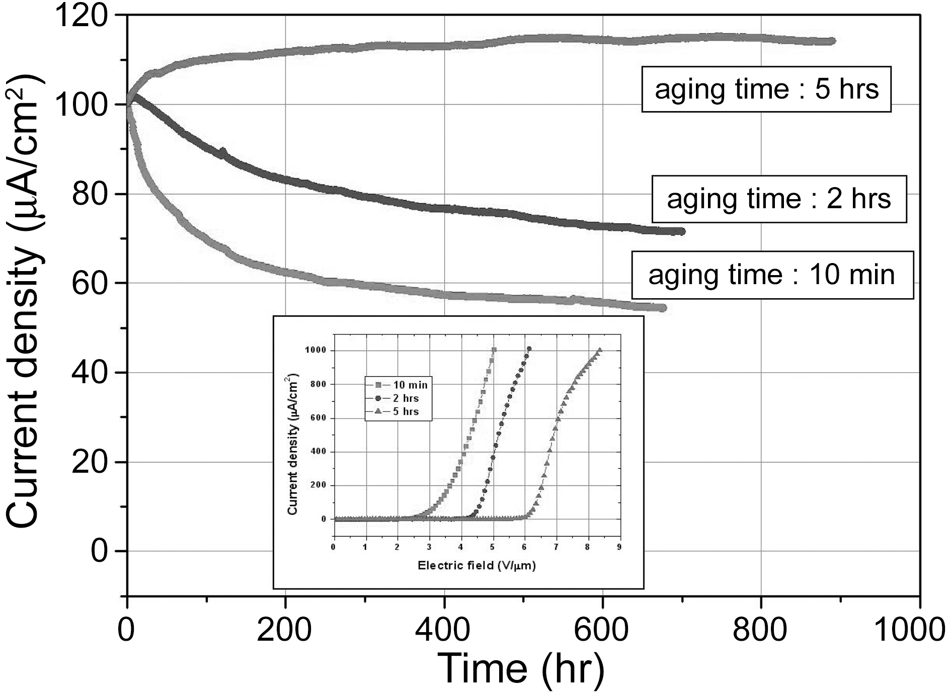
The emission stability data shown in Figs. 2 and 4 were measured with an emitter size of 2 cm×2 cm. Prior to these measurements, the emitters were electrically aged at 300 μA/cm2 with 0.1% duty ratio for 10 min. This procedure was good enough to give high stability to the emitter, as shown in Fig. 4. Since the field emission is known to be influenced by edge effect [17], we have investigated the dependence of emitter size on the stability. It was found that the stability decreased with decreasing the dimension of emitter, indicating that the
optimum aging condition varies with emitter size. It can be therefore said that one should establish the proper aging condition when a certain emitter size is designed. Fig. 5 represents the stabilities of CNT paste emitters with two different sizes (2 cm×2 cm, 0.5 cm×0.5 cm). The initial current density of 100 μA/cm2 was obtained by applying the electric fields of 3.75 V/mm and 3.25 V/mm to the emitters with sizes of 2 cm×2 cm and 0.5 cm×0.5 cm, respectively. Those two samples were aged at same condition (300 μA/cm2 with 0.1% duty ratio for 10 min). In spite of the identical aging condition, the stability of the emitter with a size of 0.5 cm×0.5 cm is much worse than that of larger emitter. This can be explained by the edge enhancement effect. The electric field is known to be enhanced at the edge of a field emitter [17,18]. It is thought that the degree of field enhancement at the edge gets larger with decreasing the emitter size since the relative portion of edge area to whole emitter size increased. It is therefore believed that the aging condition we used was affecting mostly on the edge of the small (0.5 cm×0.5 cm) emitter. The effect of aging time on the stability of the emitter was also examined. Fig. 6 shows the emission stability of CNT paste emitter (0.5 cm×0.5 cm) with three different aging times (10 min, 2 hrs, and 5 hrs). The current density and duty ratio during the aging process was 300 μA/cm2 and 0.1%, respectively. Inset in Fig. 6 shows the I-V curves of three emitters with different aging times. The emission was turned-on at the electric fields of 2.5 V/㎛, 4.3 V/㎛, and 6 V/㎛ for the emitters aged for 10 min, 2 hrs, and 5 hrs, respectively. The fields for obtaining the initial current density of 100 μA/cm2 were 3.25 V/㎛, 4.6 V/㎛, and 6.35 V/㎛. Longer aging time results in more stable emitter. As a result,the emitter aged for 5 hrs did not show noticeable decrease of current for 900 hrs of measurement time. Interestingly, the current density was increased by ~10% during the initial 100 hrs. In case of fully aged sample, there are many CNT
tips whose heights are very similar each other. At the initial stage, a certain number of CNTs are emitting 100 μA/cm2. As the heights of CNTs, which are emitting electrons, are slightly decreased by burning off, the other CNTs start to emit electrons. It is therefore believed that the emission site density was being increased during the first 100 hrs. It can be concluded that the sufficient aging process for the CNT paste emitter is necessary for the long life-time of field emission devices such as field emission display, X-ray source, and backlight for liquid crystal display.
CNT paste emitters were fabricated and then their emission stabilities were improved by post-treatments. The sealing process resulted in much higher emission stability of the emitter compared with that observed in the vacuum chamber. This phenomenon was attributed to the nonexistence of oxygen gas in the sealed device. The plasma treatment was found to improve the stability by increasing the uniformity of CNT tip heights. It was also found that the emission stability could be improved by electrical aging and the appropriate aging condition is dependent on the emitter size. This study verifies that the stability of CNT paste emitter with appropriate post-treatments is high enough to be used in field emission devices.