Since the first demonstration of efficient multilayer organic light-emitting devices (OLEDs) more than two decades ago by Tang and VanSlyke [1,2], these devices have attracted much attention for their many advantages, such as fast response time,wide viewing angle, and thin thickness for use in full color displays and lighting applications. Especially, phosphorescent OLEDs have been extensively researched because they can provide high quantum efficiency by harvesting both singlet and triplet excitons [3,4]. Cyclometalated Ir (III) complexes have been widely used as guest materials for phosphorescent OLEDs because of their highly efficient emission from mixed metal-toligand charge transfer (3MLCT) triplet states [5,6]. Since these heavy metal complexes emit light from triplet excited states by fast intersystem crossing from the singlet states, wide bandgap (Eg) materials have been used for host layers of phosphorescent devices [4-7]. Particularly, the blue phosphorescent guest molecules have high triplet energy levels (ET) so that wide Eg materials with high ET are required for efficient exothermic energy transfer from host to guest molecules. For example, N,N'-dicarbazolyl-3,5-benzene has a Eg of 3.5 eV and a ET of 2.9 eV [8,9]. N,N'-dicarbazolyl-1,4-dimethene-benzene has a Eg of 3.5 eV and a ET of 2.95 eV [10]. These wide Eg materials make carrier injection difficult, so that many organic layers are required for charge injection and transport. Furthermore, the high-energy triplet excitons generated in the emission layer of phosphorescent OLED can be diffused into the adjacent hole transport layers with lower ET levels[11], resulting in loss of excitons. Hence, complicated structures with numerous organic layers have been used for improving charge injection, transport, charge balance, and exciton confinement in blue phosphorescent OLEDs [12-15].
1,1-bis[(di-4-tolylamino)phenyl]cyclohexane (TAPC) has been widely used as a hole transport material in OLEDs because of its high hole mobility [16]. TAPC has a highest occupied molecular orbital (HOMO) energy level of 5.5 eV and lowest unoccupied molecular orbital (LUMO) energy level of 2.0 eV [17]. In addition, TAPC has a higher ET (2.87 eV) than the typical blue phosphorescent guest material, iridium (III) bis [(4,6-di-fluorophenyl)-pyridinato-N,C2'] picolinate (FIrpic) (ET of 2.62 eV) [11,18]. Therefore, TAPC can be used as a hole-transporting host material for the blue phosphorescent FIrpic guest molecules, resulting in a reduction of the number of organic layers. In this paper, we fabricated phosphorescent OLEDs with a TAPC host layer doped with FIrpic. We fabricated two kinds of simple structures, one of ITO/TAPC/TAPC:FIrpic/3-(4-biphenylyl)-4-phenyl-5-(4-tert-
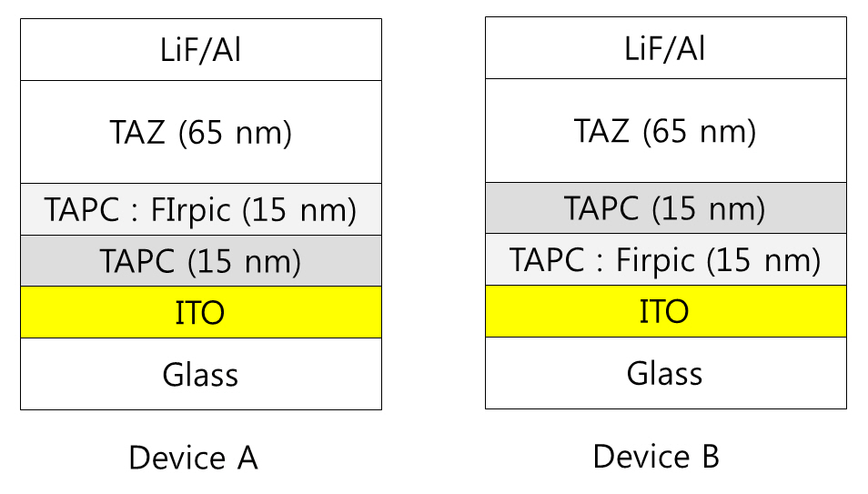
butylphenyl)-1,2,4-triazole (TAZ)/LiF/Al and the second of ITO/TAPC:FIrpic/TAPC/TAZ/LiF/Al, and investigated emission, recombination,electrical conduction, and efficiency characteristics of these devices.
Indium tin oxide (ITO) coated glass substrates were used for the preparation of the phosphorescent OLEDs with TAPC host layer. The sheet resistance of the ITO film was about 10 Ω/sq. After defining ITO anode patterns using a standard photolithography process, the substrates were cleaned with isopropyl alcohol and deionized water. All organic and metal layers were deposited using a thermal evaporation method in a base pressure of about 1 × 10⁻⁶Torr. Two kinds of organic layer structures (devices A and B) were prepared. For the device A structure, a 15 nm thick TAPC layer was deposited on the patterned ITO substrate, followed by the deposition of a 15 nm thick 2% FIrpic-doped TAPC layer. For the device B structure, a 15 nm thick 2% FIrpic-doped TAPC layer was deposited on the patterned ITO, followed by deposition of a 15 nm thick TAPC layer. Then a 65 nm thick TAZ layer was evaporated for the deposition of the electron transport layer. After depositing the organic layers, a 0.5 nm thick LiF layer and a 100 nm thick Al layer were sequentially evaporated through a shadow mask. Figure 1 shows the completed structures for devices A and B. The active area of the devices was 4 mm × 4 mm. Current density-voltage-luminance (J-V-L) characteristics of the devices were measured using computer controlled Keithley 2400 source-measure units and a calibrated fast Si photodiode. Electroluminescence (EL) and photoluminescence (PL) spectra were measured with a spectroradiometer (Minolta CS1000).
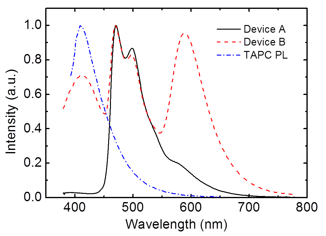
Figure 2 shows the EL spectra for devices A and B with structures of ITO/TAPC (15 nm) / TAPC:FIrpic (15 nm) / TAZ (65 nm) / LiF/Al and ITO/TAPC:FIrpic (15 nm) / TAPC (15 nm) / TAZ (65 nm) /LiF/Al, respectively. The EL peaks at 470 and 500 nm are attributed to the radiative transition from the blue phosphorescent guest (FIrpic) molecules [18]. The peak at 470 nm originates from mixed 3MLCT states, whereas the peak at 500 nm is due to the π-π* transitions [19]. In addition to the emission from FIrpic, device A exhibits another emission shoulder at about 590 nm for the emission from TAPC molecules [20]. The TAPC molecules are composed of tri-p-tolylamine (TTA) moieties [20]. The emission at 590 nm is ascribed to the direct cross-radiative recombination of electrogenerated TTA ion pairs [21]. The 590 nm emission is not observed in the PL spectrum of the TAPC molecules, since this emission originates from TTA ion pairs generated by the ap-
applied electric field [20]. The cross recombination on the TTA+-TTA- ion pairs depends on the electric field [22]. Another feature in the EL spectra of device A is the emission below 450 nm. This emission intensity does not approach zero, even at low voltage. This might be due to emissions from TAPC singlet excited states. Such emissions can be clearly seen in the EL spectra of device B. Device B exhibits additional strong emissions at about 410 nm in addition to the peaks due to the FIrpic and TTA ion pairs. This emission coincides with the PL spectrum of TAPC measured in tetrahydrofuran solution, as seen in Fig. 2. It indicates that the emission at about 410 nm results from the radiative decay of TAPC singlet excited states. It has been reported that the excimeric states can be created in the solid-state TAPC layer[20], resulting in the radiative emission at about 450 nm in the spectrum. However, this excimeric emission is not observed in device B, as seen in Fig. 2. In addition to the TAPC singlet emission, device B exhibits strong emission intensity at 590 nm owing to the TTA ion pairs of TAPC molecules, the intensity of which is substantially higher compared with device A. Hence, device B exhibits whitish emission with the Commission Internationale de l’Eclairage (CIE) coordinates of (0.353, 0.326). Therefore, these results indicate that the recombination zone in device B is located within the undoped TAPC layer inserted between the doped TAPC and TAZ layers. Similarly, the strong FIrpic emission in de-
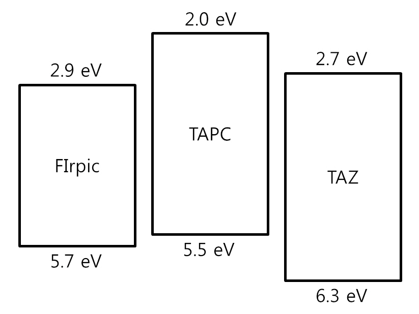
vice A suggests that the recombination takes place in the doped TAPC layer adjacent to the TAZ layer. This can be supported by the HOMO and LUMO energy diagram shown in Fig. 3. TAPC has HOMO and LUMO levels of 5.5 and 2.0 eV, respectively [17]. On the other hand, TAZ has HOMO and LUMO levels of 6.3 and 2.7 eV, respectively [23]. Hence, the energy barrier for hole injection into TAZ from TAPC is 0.8 eV at the interface between the TAPC and TAZ layers, whereas the barrier for electron injection into TAPC from TAZ is 0.7 eV. In addition, the hole mobility of TAPC is about three orders of magnitude higher than the electron mobility of TAZ [16,24]. Therefore, most holes are confined within the TAPC layer adjacent to the TAZ layer. However, some holes overcome the energy barrier at the interface and recombine with electrons in the TAZ layer, resulting in weak emissions from TAZ. The combination of weak emissions from TAPC and TAZ singlet excitons results in a weak plateau in the 380 nm to 450 nm region in the EL spectrum of device A.
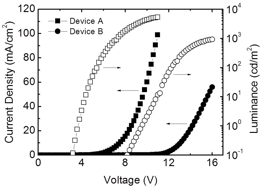
Figure 4 shows the J-V-L curves for devices A and B. The driving voltage of device A is lower than that of device B. For example, device A exhibits a current density of 20 mA/cm2 at an applied voltage of 8.4 V. On the other hand, device B requires a voltage of 13.8 V to obtain the same current density. With regard to luminance, device B also requires a higher voltage to obtain the same results. For example, the threshold voltage, which is defined as the voltage required for a luminance of 1 cd/m2, is 3.8 V in device A, and 9.6 V in device B. The voltages for luminance of 100 cd/m2 are 5.4 and 12.2 V for devices A and B, respectively.
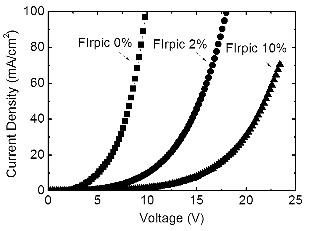
Since the recombination zone is near the interface between the TAPC and TAZ layers, it can be suggested that FIrpic molecules in the TAPC layer may impede hole conduction. In order to investigate the effect of FIrpic on hole conduction in the TAPC layer, TAPC hole-only devices were fabricated with a structure of ITO/TAPC:FIrpic (100 nm, x%)/Al, where the concentration of FIrpic (x%) was varied to 0%, 2%, and 10%. In these devices, the barrier for hole injection is about 0.5-1.0 eV depending on the work function of ITO [25], whereas the electron injection barrier is about 2.2 eV. Therefore, the large energy difference between the electron and hole injection barriers makes these hole-only devices. Figure 5 shows the J-V curves for the hole-only devices. The voltage to obtain the same current density increases as doping of the FIrpic molecules into the TAPC layer increases. For example, the undoped TAPC hole-only device requires an applied voltage of 6.4 V to obtain a current density of 20 mA/cm2. However, 2% and 10% FIrpic-doped devices require higher voltages of 12.2 V and 18.4 V, respectively, for the same current density. These results indicate that the FIrpic molecules in TAPC impede hole conduction in TAPC. Since the HOMO level of FIrpic is deeper than that of TAPC, as seen in Fig. 3, it can be postulated that the possible trapping of holes on the FIrpic molecules is not significant in the FIrpic-doped TAPC layer. The FIrpic molecules may decrease the hopping possibility by increasing the hopping distance between TAPC molecules [26].
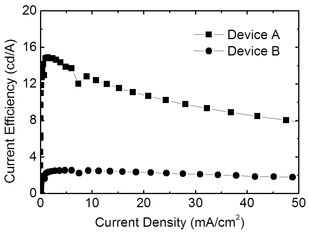
Figure 6 shows the current efficiency curves as a function of current density for device A and device B. Devices A and B exhibit maximum current efficiencies of 15 cd/A and 2.6 cd/A, respectively. The maximum current efficiency of device A is about 5.8 times higher than that of device B. Because the current efficiency of the device depends on charge balance and emission efficiency of excitions, assuming the same outcoupling conditions,a bilayer device with a structure of ITO/TAPC:FIrpic (30 nm, 2%)/TAZ (65 nm)/LiF/Al was prepared to investigate the origin of efficiency differences between devices A and B. The bilayer device exhibited a maximum current efficiency of 23 cd/A. In this bilayer device, the charge balance may be similar to that of device B, since the doping of FIrpic molecules into the entire TAPC layer may not seriously modify the hole injection and transport conditions compared with those of device B. Therefore, lower efficiency in device B may result from low emission efficiency of the excitons generated in the TAPC host layer. As shown in Fig. 2, most of the emissions in device A come from the triplet excited states of the phosphorescent guest (FIrpic) molecules. However, in device B, both the TAPC singlet excitons and the direct cross recombination on the TTA ion pairs strongly contribute to the current efficiency. Therefore, these results suggest that emission from the direct cross recombination on the TTA ion pairs is not efficient.
The electrical and optical properties of device A (ITO/TAPC/TAPC:FIrpic /TAZ/LiF/A) and device B (ITO/TAPC:FIrpic/TAPC/TAZ/LiF/Al) have been investigated. As recombination took place in the TAPC host adjacent to the TAZ layer, device B exhibited strong emission intensities from TAPC singlet excitons and direct cross-radiative recombination on the TTA ion pairs in the TAPC layer. These emissions from the TAPC layer made device B be whitish with Commission Internationale de l'Eclairage (CIE) coordinates of (0.353, 0.326). The emission by these TAPC singlet and TTA ions pairs also resulted in the low current efficiency in device B. On the other hand, the higher current efficiency in device A resulted from the phosphorescent emissions from FIrpic molecules, which are doped into the TAPC host. The driving voltage of device A was lower than that of device B, as the FIrpic molecules in TAPC decreased hole conduction in the TAPC layer.