In order to improve efficiency and make a new material thin film, we prepared the Al-In-Sn-ZnO thin film on a glass substrate at room temperature using a Facing Target Sputtering (FTS) system. The FTS system was designed to array two targets that face each other. Two different kinds of targets were installed on the FTS system. We used an ITO(In2O3 90wt%, SnO2 10wt%) target and an AZO (ZnO 98wt%, Al2O3 2wt%) target. The AIZTO films were deposited using different applied powers to the targets. The as-deposited AIZTO thin films were investigated using a UV/VIS spectrometer, an X-ray diffratometer (XRD), and Energy Dispersive X-ray spectroscopy (EDX).
The importance of transparent electrodes is growing due to the rapid development of displays and, accordingly, many studies are underway on transparent conducting oxide (TCO) thin films. The TCO materials that are currently widely used are indium tin oxide (ITO), aluminum zinc oxide (AZO), indium zinc oxide (IZO) and gallium zinc oxide (GZO). These materials consist of three elements, and attempts are being made to improve their properties. Due to research into sputtering methods and multilayers, the properties of transparent electrodes have been improved, but these methods of deposition have drawbacks,such as their high cost and longer fabrication time. Among the widely used TCO materials, ITO has high transmittance and low resistance [1], while AZO has high stability in a hydrogen plasma and a low growth temperature [2] so they are both widely used as transparent electrodes for flat panel displays, solar cells, and organic light emitting devices (OLEDs).
However, ITO and AZO have defects that interfere with their use as transparent electrodes. The former has problems with instability in a hydrogen plasma and is toxic [3], while the latter has a lower electrical conductivity than the former [4].
Therefore, new materials and sputtering methods are needed to improve efficiency of transparent electrodes and complement the shortcomings of these electrode materials.
In this study, we prepared Al-In-Sn-ZnO thin films with a different ingredient ratio by using a facing targets sputtering (FTS) system with ITO and AZO as the targets, and then examined their properties.
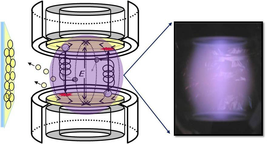
For the deposition of the films, we first cleaned the substrate to remove the surface impurities. The substrate was ultrasonically cleaned with de-ionized water (D.I. Water) for 20 minutes and isopropyl alcohol (IPA) for 20 minutes and then dried with N2 gas. In this experiment, we prepared the AIZTO thin films by using a facing targets sputtering (FTS) system (as shown Fig. 1).
In the case of general magnetron sputtering systems, the substrate and the as-prepared thin film are placed in the space where they will be exposed to the plasma. Therefore, there is a limitation to the production of high quality thin films because damage caused by bombardment with high-energy particles, such as oxygen ions, is inevitable. However, in this study, a new type of thin film was prepared using the FTS system due to the two target structure used. By applying various power levels to the two targets, the FTS system can control the ingredient ratio of the thin films.
For this reason, the FTS system can prepare thin films with various ingredient ratios and new materials of various properties
[Table 1.] Sputtering Condition.

Sputtering Condition.
with fixed ingredient ratios. The substrate is located in a plasmafree area away from the center of the plasma, thus suppressing the high energy particle bombardment of the substrate. Also, because of the cathode electric potential of facing targets, the relectron reciprocates target to target and makes the reactive gas ionization higher. Therefore, the FTS system can prepare high quality thin film at a low gas pressure. We used glass substrates and a thickness of thin film fixed at 100nm at room temperature
during the experiment. The detailed experimental conditions are shown in Table 1. The electrical and structural properties of the as-deposited AIZTO thin films were then examined by hall-effect measurement, and by using an atomic force microscope (AFM), an X-ray diffractometer (XRD), and energy dispersive x-ray spectroscopy (EDX). The optical properties were measured by an UVVIS spectrometer.
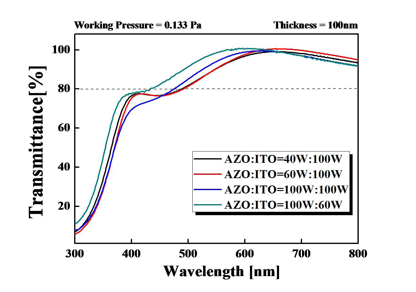
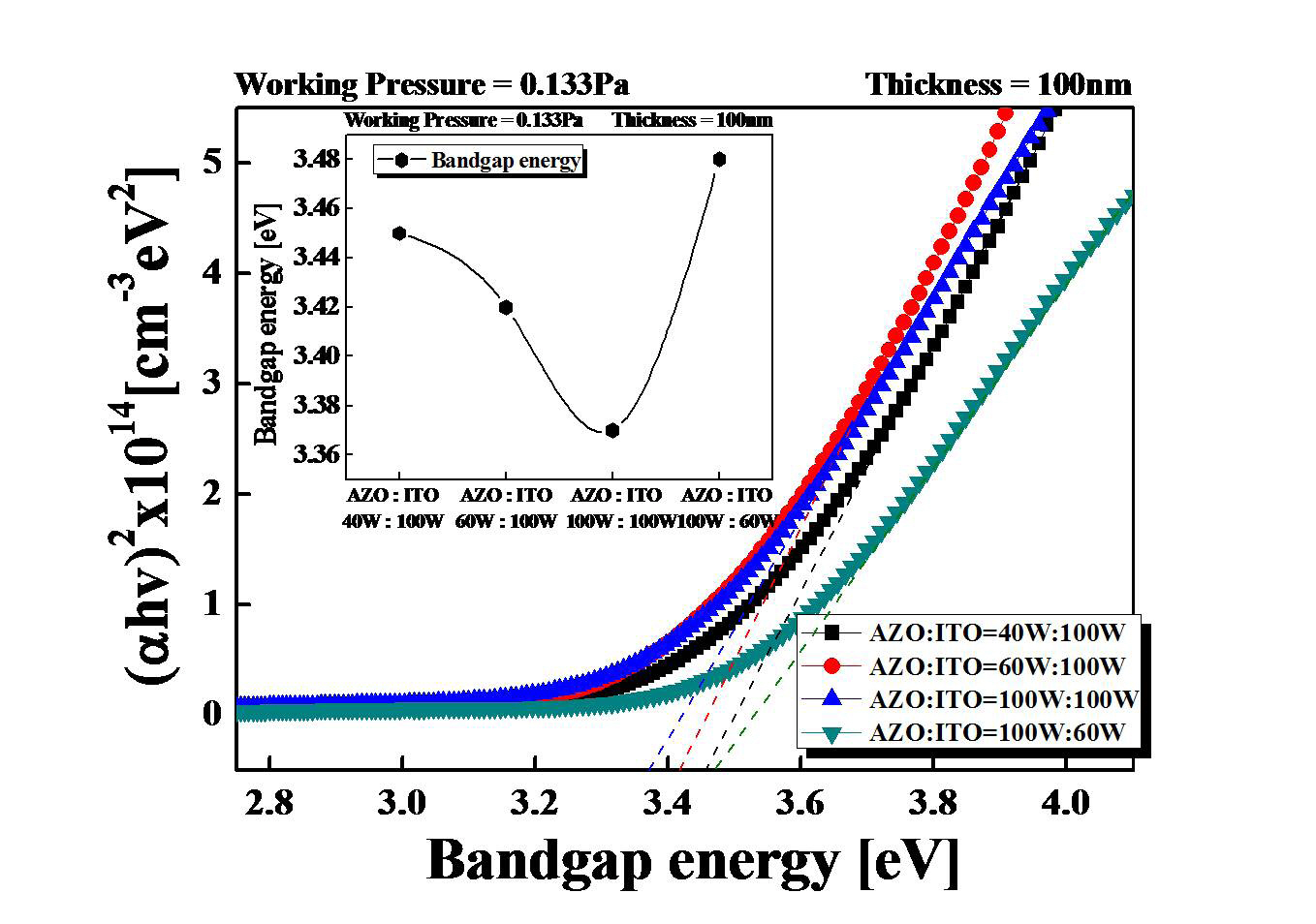
Figures 2 and 3 show the optical transmittance and the optical band gap energy of the AIZTO thin films as a function of the input power, respectively. According to the recently reported study results, the AZO and the ITO thin films had a transmittance of 80% [5]. However, all of the deposited-AIZTO thin films in this study showed a greater than 85% and a band-gap energy greater than 3.3 eV in the visible range. As shown Figure 2, we observed a shift of the absorption region of the AIZTO thin films with increasing input power. This Burstein-Moss shift was caused of the carrier concentration change [6].
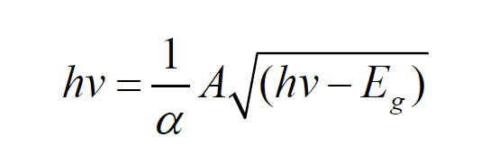
In the absorption region, the optical band-gap energy could be calculated by the following formula:
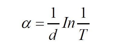
where d is the thickness of the film and T is the transmittance. α2 is plotted as a function of the photon energy:
As the input power of the AZO thin film increased, the optical band-gap energy decreased and shifted.
As the AZO input power increases, ratios of the AZO atomic configuration are increases. Therefore, the concentration of electrons will be reduced and the optical band-gap energy is decreased, because the electrons cannot become degenerate in the conduction band. In other words, because of the decrease in the electron concentration, due to the various materials in the AIZTO thin film, the optical band-gap energy was decreased [7].
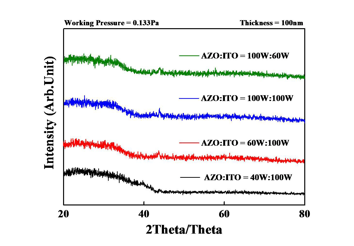
Figure 4 shows the X-ray diffraction (XRD) pattern of the AIZTO thin films as a function of the input power. We observed amorphous property in the deposited AIZTO thin films. In the preceding experiment, peaks were observed in the XRD patterns of the as-deposited and annealed AIZTO thin films with sufficient thickness. However, in this study, AIZTO thin film showed amorphous. The reason for this was that the AIZTO thin film was too thin and the energy required for crystallization is undersupply.
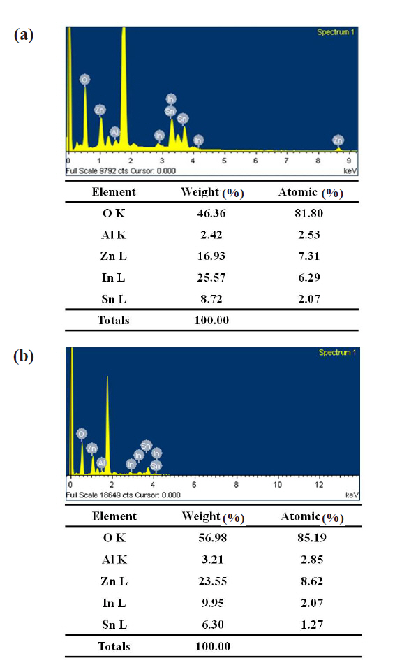
Figure 5 shows the energy dispersive x-ray spectroscopy (EDX) image of the AIZTO thin films as a function of the input power. We observed a change in the component ratio of the AIZTO thin films as function of the input power. Based on these results, it is expected that thin films with various properties can be prepared by controlling the ratio of atomic concentrations while keeping the component ratio of the target fixed.
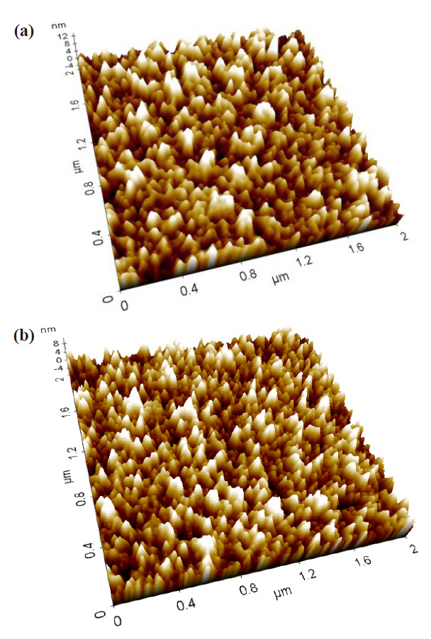
Figure 6 shows the atomic force microscope (AFM) image of the AIZTO thin films as a function of the input power. The RMS (root-mean-square) value of the AIZTO thin films showed an approximately 1.7 nm of surface roughness. The RMS values of the AIZTO thin films were less than the surface roughness of conventional ITO thin films (2 nm), indicating that they had a smooth surface [8]. Due to this surface smoothness, it though that the AIZTO thin films are suitable for an organic light emitting device (OLED) anode.
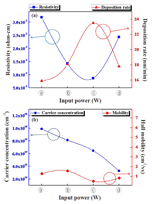
Figure 7 shows the electrical properties of the AIZTO thin films as a function of input power. The AIZTO thin films showed the highest deposition rate (23.6 nm/min) and lowest resistivity (8.54× 10⁻³ Ω-cm) at an input power of 100W for each of the targets. With an increase of the input power on the AZO target the deposition rate increased and the carrier concentration decreased.
The properties of the AZO thin films are known to be dependent on the oxygen content, so the electrical properties of the AZO thin film are dependent on its oxygen contents [9]. Therefore, the resistivity and carrier concentration are affected by the ratio of the atomic concentration of AZO and increased in the deposited-AIZTO thin film.
For this reason, it is thought that the electrical properties of the AIZTO thin films were changed by the change in the component ratio change due to the variation the input power.
In this study, we prepared Al-In-Sn-ZnO (AIZTO) thin films on glass substrates at various input power using a FTS system. The properties of the AIZTO thin films with various component ratio achieved by changing the input power of AZO and ITO were evaluated. As a result, changes were observed in the component ratio by changing the input power, and a smooth surface was obtained. The as-deposited-AIZTO thin films showed a resistivity of 8.54 × 10⁻³ Ω-cm and a high transmittance, above 85%, in the visible range. We surmise that AIZTO thin films can be prepared with improved properties by changing the sputtering conditions.