As the complementary metal-oxide semiconductor (CMOS)technology progresses into the 22 nm regime, the fundamental limitations of silicon are felt stronger. New superior materials are needed to achieve higher performance and scalable CMOS integrated circuits in the future. Carbon-nanotube (CN) transistor is a promising candidate for replacing silicon metal oxide semiconductor field effect transistor (Si-MOSFET) [1-6]. CN transistors display desirable characteristics such as elastic carrier scattering,ballistic carrier transport, and smaller device footprint (area) as compared to conventional Si-MOSFETs [1].
Two types of CN transistors have recently attracted significant attention in the literature: Schottky Barrier (SB) controlled switch (CN-SBFET) and MOSFET-like switch (CN-MOSFET) [1-6]. CNSBFETs are formed by directly attaching the intrinsic nanotube channels to the metal source/drain contacts. CN-SBFETs show ambipolar carrier transport. Alternatively, the CN-MOSFET displays unipolar behavior with heavily doped source and drain extension regions. A coaxial gated CN-SBFET and a CN-MOSFET are compared in [2]. CN-MOSFETs produce higher on-state and lower leakage currents. By providing a significantly higher Ion/Ioff ratio, CN-MOSFETs display better scalability as compared to CNSBFETs. CN-MOSFET is the focus of the study presented in this paper due to the superior performance as compared to the CNSBFET.
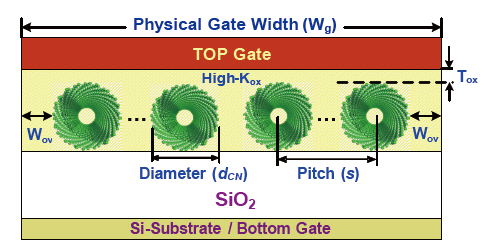
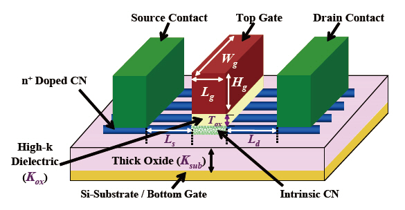
The structure of a planar-gated N-type CN-MOSFET is shown in Fig. 1. The CNs are heavily doped with donors (n+) in the source and drain extension regions in an N-type CN-MOSFET. The nanotubes are undoped under the gate. The cross-sectional view of a CN-MOSFET is shown in Fig. 2. Multiple nanotubes are placed in parallel to form an array that produces sufficient current with a CN-MOSFET.
Inspired by the developments in CN related research, publications on novel circuit techniques for very large scale integration (VLSI) of CN-MOSFETs have recently started to appear in literature [7-11]. All of these studies are based on Stanford CN-MOSFET HSPICE compact model [12]. A multithreshold voltage six-transistor (6-T) static random access memory (SRAM) cell using CN-MOSFETs is presented by Lin et al. in [7] to provide higher performance as compared to the 32 nm-Si-MOSFET based memory cells. The characteristics of 6-T CN-MOSFET and Si-MOSFET SRAM cells are compared by Moradinasab et al. in [8] assuming a 32 nm CMOS technology. A new CN-MOSFET SRAM cell is proposed by Ebrahimi and Afzali-Kusha in [9] to enhance the read static noise margin as compared to a conventional Si-MOSFET memory cell. A novel eight-transistor CN-MOSFET SRAM cell is proposed by Kim et al. in [10] to lower the dynamic switching power consumption
as compared to silicon FinFET memory circuits. A new ternary inverter is proposed by Lin et al. in [11] for lower power consumption and higher performance with the CN-MOSFET technology. The conclusions of these recent publications are however difficult to reproduce and verify. Unlike a Si-MOSFET, device size is not determined merely by the physical gate width and channel length in a CN-MOSFET. The complex relationship between device sizing and performance due to the unique material properties and nanotube array structure of a CN-MOSFET is typically overlooked in these previous publications. Device and circuit design options such as transistor sizing (number of tubes), carbon nanotube array physical structure (nanotube diameters and pitch), and choice of substrate voltage are not discussed in sufficient detail.
A thorough understanding and a careful optimization of the device structure are essential to be able to develop high-performance integrated circuits with CN transistors. A p-channel CNMOSFET device profile optimization study for achieving highspeed carbon nanotube integrated circuits is presented in [13]. Alternatively, the electrical characteristics of 16 nm N-type CNMOSFETs are explored from a circuit designer’s point of view in this paper. The purpose of this paper is to bridge the fledgling CN-MOSFET based novel circuit development and VLSI efforts to the underlying emerging CN technology. The optimization study is based on the Stanford CN-MOSFET HSPICE compact model [12]. The dependence of device performance on the physical geometry of carbon nanotubes is presented. The optimum high-performance device profiles that provide the maximum Ion/Ioff ratio are identified. Technology development and utilization guidelines are provided to achieve high-speed, low-leakage, area efficient, and manufacturable integrated circuits with CN field effect transistors.
The paper is organized as follows. The performance-critical parameters in the physical structure of a CN-MOSFET are highlighted in Section 2. The optimization results with technology development and utilization guidelines for high-performance 16 nm N-type CN-MOSFETs are presented in Section 3. Finally, some conclusions are offered in Section 4.
2. IMPORTANT CN-MOSFET PARAMETERS
Important device parameters for modeling and performance characterization of CN-MOSFETs are highlighted in this section. The relationships among CN diameter, energy bandgap, Ion, and Ioff in a CN-MOSFET are explained in Section 2.1. The distinctions among the physical gate width, physical channel width, and effective channel width in a CN-MOSFET are described in Section 2.2. The important set of physical parameters from the 16 nm CN-MOSFET technology considered in this performance optimization study is presented in Section 2.3.
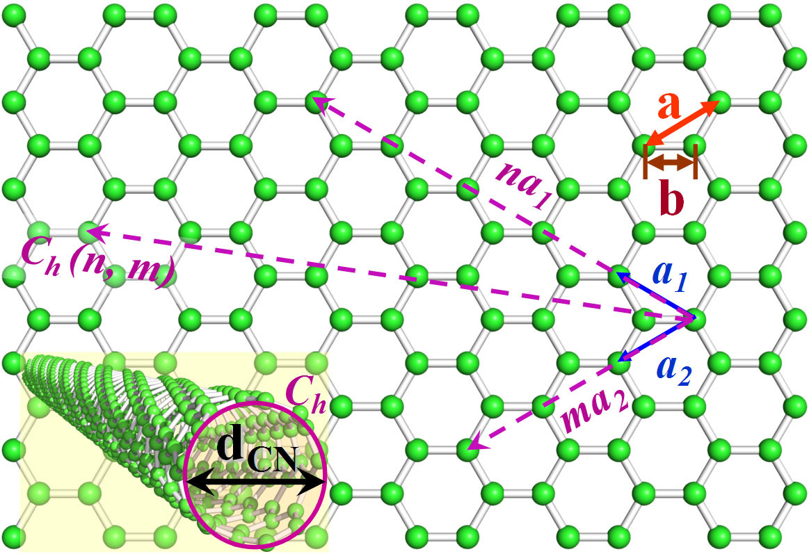
The diameter of a single-walled CN (SWCN) is specified by the chirality vector
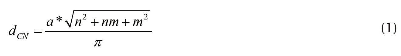
where
The energy bandgap (
The channel is a doped single piece of silicon extending between the source and drain terminals in a Si-MOSFET. The gate width is essentially the length of the (polysilicon or metal) gate that overlaps the channel area perpendicular to the direction of current flow between the source and drain in a Si-MOSFET. The definition and measurement of the gate width are however different in a CN-MOSFET. Unlike a Si-MOSFET, the channel of a CN-MOSFET is composed of an array of discrete nanotubes
[Table 1.] Set of process parameters for 16 nm N-type CN-MOSFET.
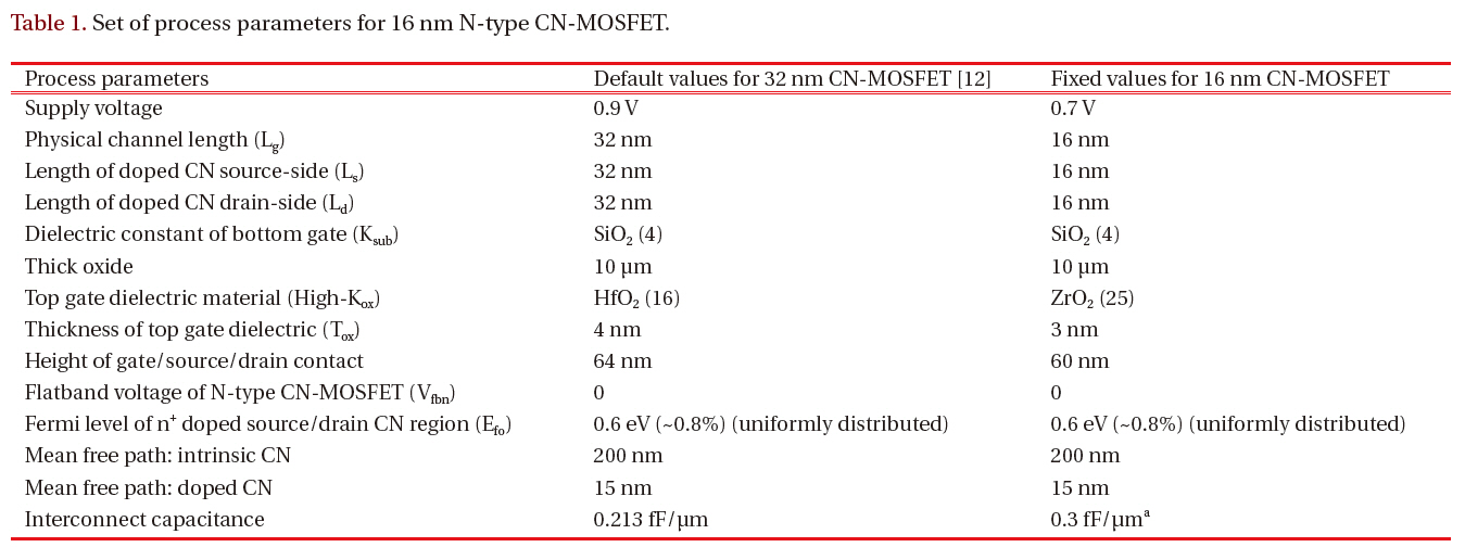
Set of process parameters for 16 nm N-type CN-MOSFET.
separated by insulator as illustrated in Fig. 2. The gate width of a CN-MOSFET can be therefore defined in three different ways.
The total area of a CN-MOSFET is determined by the physical gate width (

where N is the number of tubes in a CN-MOSFET. Inter-tube pitch (
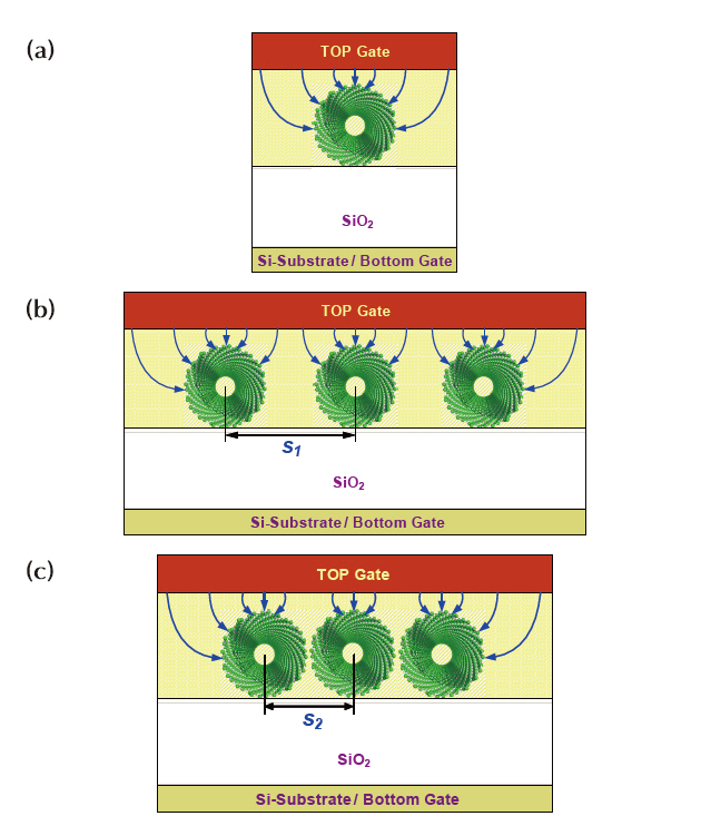
A single CN typically provides a limited amount of current. An array of multiple nanotubes is therefore necessary to be able to produce sufficient drain-to-source current in a CN-MOSFET. The physical channel width (
The electric field lines emerging from the gate terminal terminate on the CNs that form the channel. These electric field lines penetrating into the channel area are screened by the neighboring insulated nanotubes. When a positive voltage is applied on the gate terminal of an N-type CN-MOSFET, the charge induced on the CNs interact as illustrated in Fig. 4. The gate-to-channel capacitance and the resulting current produced by a nanotube are reduced due to enhanced screening effect with decreased inter-tube spacing (pitch). Charge screening reduces the effective width of the channel, thereby degrading the device current [16, 17]. Considering the charge screening effect, the effective channel width (
where α is the screening effect coefficient (0< α ≤ 1). When there is only one tube per gate, α = 1. For N > 1, α is primarily
determined by the nanotube pitch. Screening effect is also influenced by the CN diameter, the number of tubes, the supply voltage,and the channel length of the device.
The current produced by a CN-MOSFET is determined by the effective channel width
2.3 Device scaling and parameter settings
The fixed (not considered for optimization) process parameters of the 16nm CN-MOSFETs in this study are listed in Table 1. The ‘Default value for 32 nm CN-MOSFET’ column includes the default device parameters of the 32 nm Stanford University CNMOSFET technology presented in [12]. As listed in Table 1, the interconnect capacitance increases when the channel length is scaled [16]. High-performance nanotube transistors with integrated high-k (~25) dielectrics (zirconium oxide thin-films)are described by Javey et al. in [18]. A high-k gate oxide material (ZrO2) with a dielectric constant of 25 and a nominal thickness of 3 nm is assumed here to achieve high-speed transistors.
3. OPTIMIZATION OF N-TYPE CN-MOSFET
The current produced by a CN-MOSFET depends on important physical parameters such as the diameters of nanotubes, the inter-tube pitch, and the number of tubes. These parameters determine the effective channel width and device strength.In this section, the CN diameters are optimized to maximize the Ion/Ioff ratio for different nanotube arrays with different effective device channel widths. The influence of inter-tube pitch on device performance is evaluated with two different substrate (bottom-gate) voltages. The design tradeoffs among Ion, Ioff, and Ion/Ioff for N-type CN-MOSFETs are presented. All of the nanotubes are assumed to be semiconducting with uniform intertube pitch. Imperfections such as diameter variations and metallic nanotubes during the manufacturing of CN-MOSFETs are not considered in this paper. The die temperature is assumed to be 90℃ [20]. The nominal supply voltage is 0.7 V. The channel lengths of all the CN-MOSFETs considered in this paper are 16 nm (Lg = 16 nm).
3.1 Nanotube diameter optimization
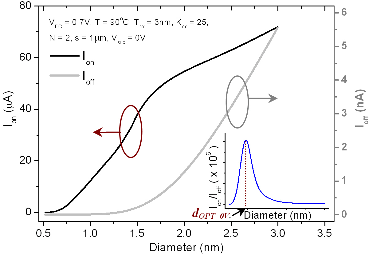
In this section, the diameter of carbon nanotubes is optimized to achieve the maximum Ion/Ioff ratio. Ion is the drain current at VGS= VDS = VDD = 0.7 V. Ioff is the subthreshold leakage current at VGS =0 V and VDS = VDD = 0.7 V.
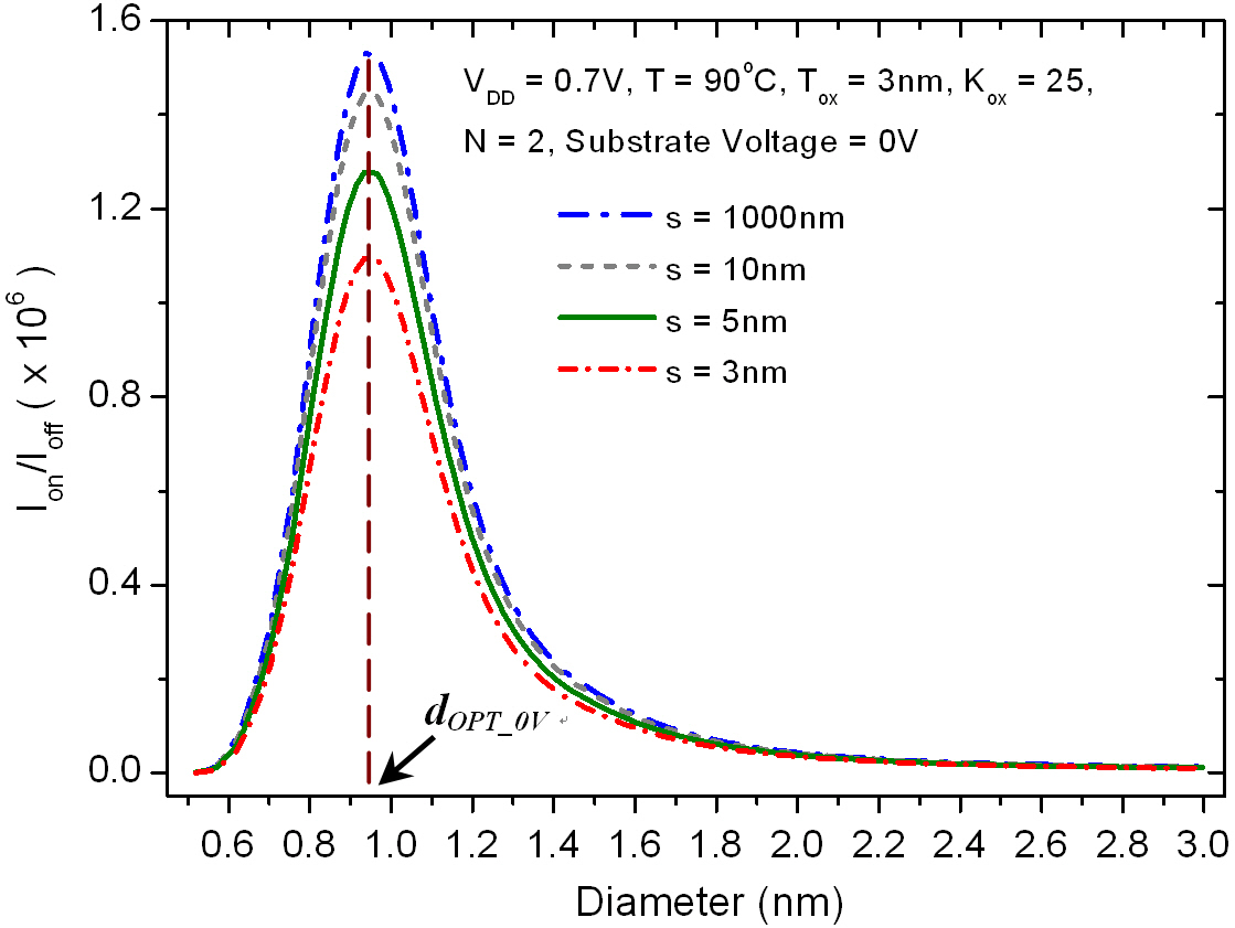
In order to evaluate the dependence of Ion and Ioff on the diameter of nanotubes, an N-type CN-MOSFET with 2 tubes is presented as an example next. As discussed in Section 2.2, nanotube array pitch has a strong influence on Ion produced by a CN-MOSFET. Similarly, the maximum achievable Ion/Ioff is affected by the array pitch. The optimum nanotube diameter that maximizes Ion/Ioff however is insensitive to the nanotube array pitch. The inter-tube pitch (s) is assumed to be 1 ㎛ in this section to effectively eliminate the charge screening effect(i.e., α 1) and determine the maximum Ion/Ioff achievable with a CN-MOSFET. The maximum performance provided by an ideal CN transistor that does not suffer from charge screening effect is identified. The range of nanotube diameters is from 0.5 nm to 3 nm. All the possible chirality vectors (n, m) that can produce the diameters in this range are considered in this study.
For a fixed number of tubes and a fixed pitch, enlarging the CN diameter enhances both Ion and Ioff as shown in Fig. 5. The increased diameter decreases the resistance of the channel region. The source and drain resistances are also reduced due to the higher number of carriers induced in the semiconducting subbands as the diameter is enlarged. The variation of Ion is primarily
due to the strong modulation of the source and drain resistances with the CN diameter [21].
Subthreshold leakage current is exponentially increased with the diameter. Ioff is controlled by the energy bandgap (Eg) of CNs. Ioff is dominated by the band-to-band tunneling current in a CNMOSFET[2]. The energy bandgap of CN is reduced as the diameter is increased. In the subthreshold region, particularly when a negative gate voltage is applied to an N-type CN-MOSFET, the band-to-band tunneling current is enhanced with increased diameter. The additional band-to-band leakage current (Ibtbt) through the semiconducting sub-bands is particularly severe for high VDS in a CN-MOSFET [21].
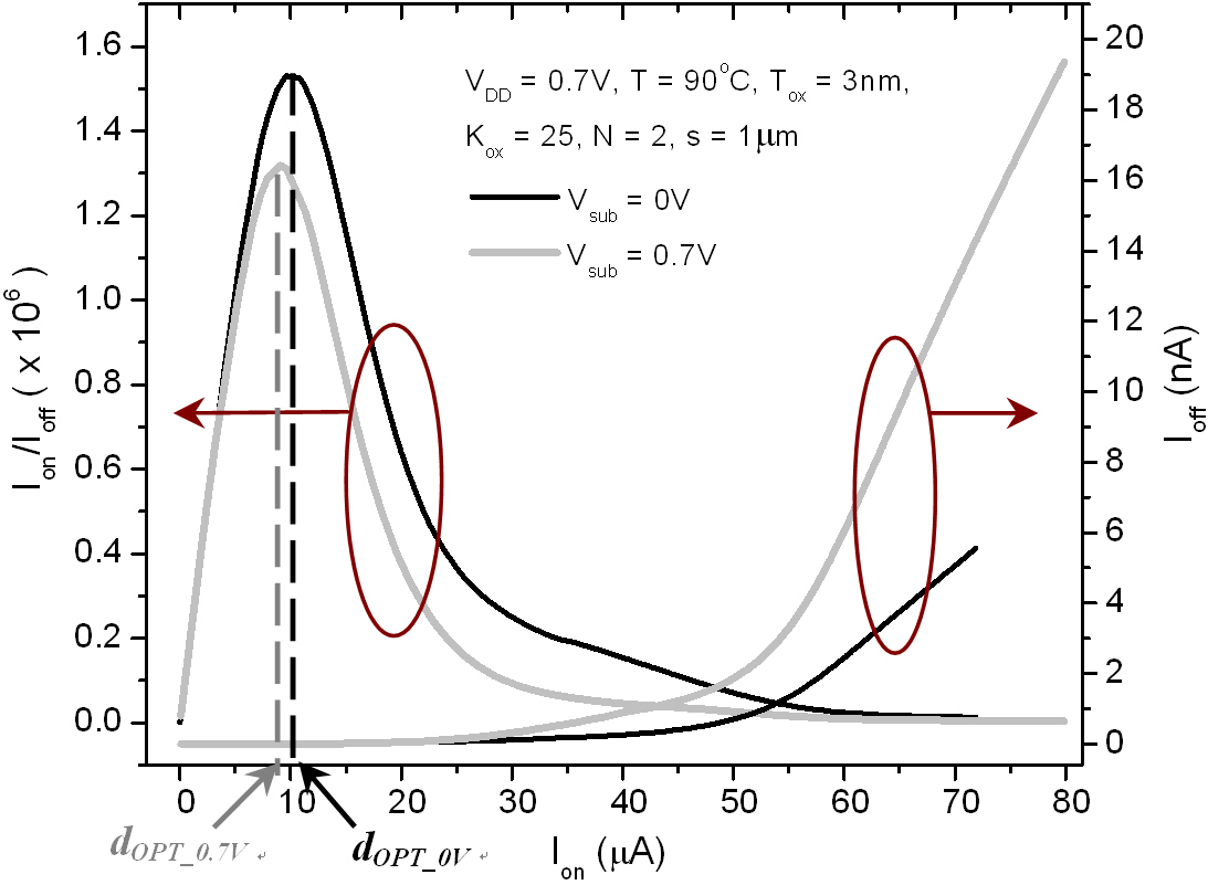
When the diameter (
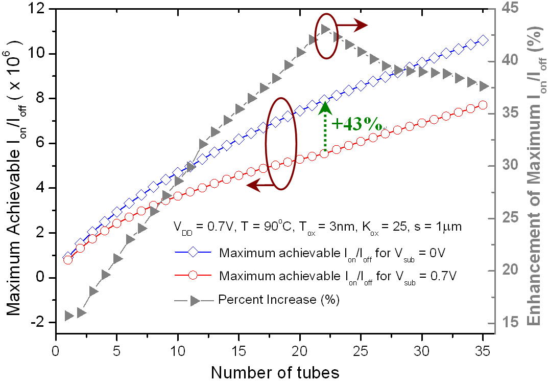
The substrate can be viewed as a second (bottom) gate below a thick oxide layer in a CN-MOSFET [12]. Ion is enhanced due to stronger channel inversion with a higher substrate voltage. The subthreshold leakage current however is also increased when the substrate voltage is higher than 0 V. An n-channel CN-MOSFET cannot be effectively cut-off provided that the substrate is connected to the power supply (Vsub = VDD = 0.7 V). The maximum achievable Ion/Ioff and the corresponding optimum nanotube diameter are therefore reduced with a higher substrate voltage.
The variation of maximum achievable Ion/Ioff with the number of tubes (1 ≤
3.2 The effect of substrate voltage on the optimum diameter
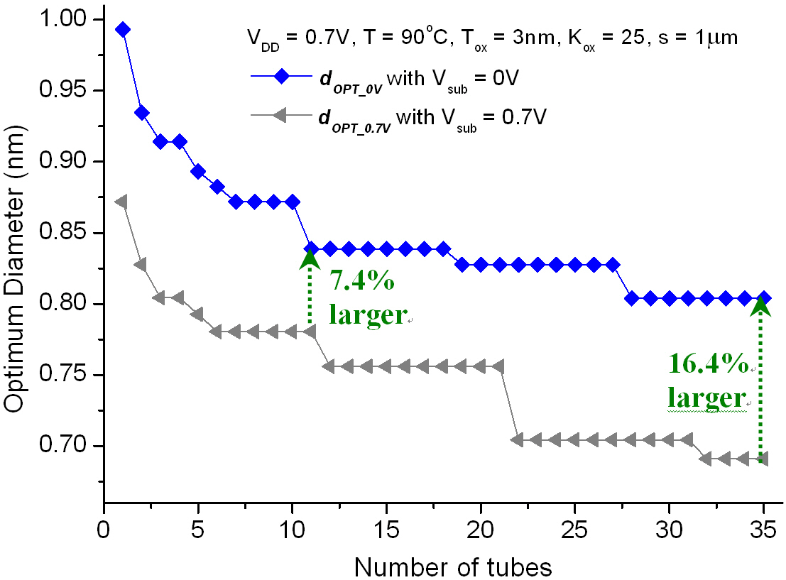
The variation of optimum nanotube diameter with the transistor size (number of tubes) for Vsub = 0 V and Vsub = 0.7 V is shown in Fig. 8. Both
0.993 nm to 0.804 nm (a reduction of approximately 23%) with the increased transistor size (as
In addition to enhanced Ion/Ioff, the optimum nanotube diameter that maximizes Ion/Ioff is also enlarged with a smaller substrate voltage. For 1 ≤
3.3 Device performance versus integration density tradeoffs
The ideal maximum Ion/Ioff of an optimized N-type CN-MOSFET is achieved at a high inter-tube pitch (assumed to be 1㎛ in Section 3.1) where the screening effect is negligible. This pitch is however impractically long from an area efficiency point of view. Shorter pitches are desirable to enhance the integration density of a chip with CN-MOSFET technology. In this section, the effect of pitch reduction on the maximum achievable Ion/Ioff is evaluated.
As shown in Fig. 9 with
As
2 and 3. There is therefore a tradeoff between switch performance (Ion/Ioff) and area efficiency (
3.4 Uniform nanotube diameter for manufacturability with different transistor sizes
As shown in Sections 3.1 and 3.2, Ion/Ioff can be maximized by manufacturing nanotubes with carefully optimized diameters
The optimum diameter for achieving the maximum Ion/Ioff varies with the number of tubes (transistor size) as shown in Fig. 8.
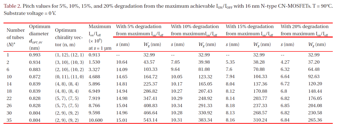
Pitch values for 5% 10% 15% and 20% degradation from the maximum achievable ION/IOFF with 16 nm N-type CN-MOSFETs. T = 90℃. Substrate voltage = 0 V.
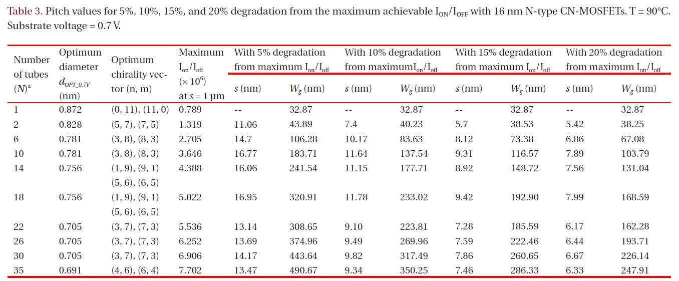
Pitch values for 5% 10% 15% and 20% degradation from the maximum achievable ION/IOFF with 16 nm N-type CN-MOSFETs. T = 90℃. Substrate voltage = 0.7 V.
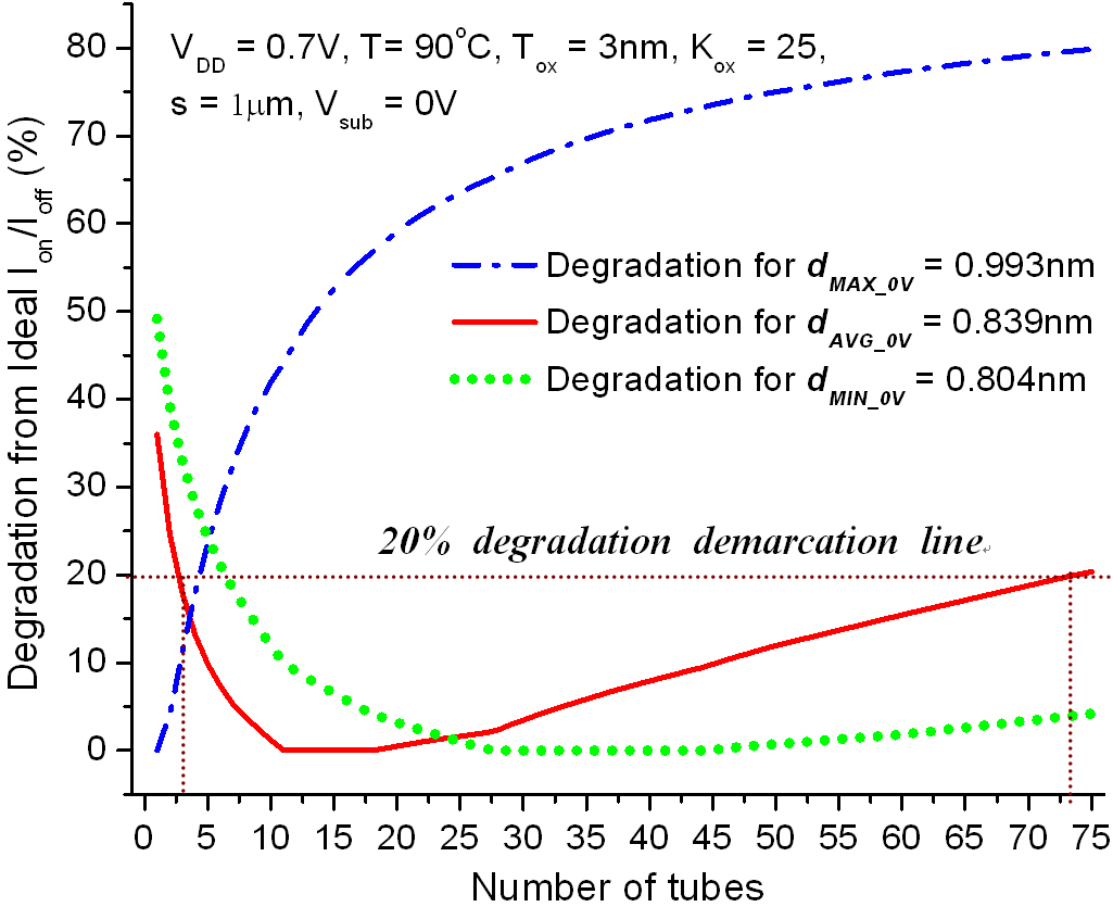
Fabricating nanotubes with different diameters for various sizes of CN-MOSFETs on a complex chip is not practical. For low-cost and high-yield manufacturability, it is highly desirable to have only one uniform nanotube diameter (for a single-Vth CN-MOSFET technology) across a chip. The effect of a uniform diameter on the performance of various sizes of CN-MOSFETs is evaluated in this section. 35 different transistor sizes are considered (the number of tubes is varied from 1 to 35) to determine a single uniform and manufacturable diameter with acceptable degradation from the ideal switch performance.
Three possible uniform diameters are evaluated for various sizes of CN-MOSFETs. The average diameter (
The degradation from the ideal maximum Ion/Ioff (observed at
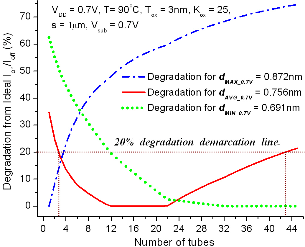
Similar analysis is also conducted to determine a practical uniform diameter for which the Ion/Ioff degradations are smaller than 20% at Vsub = 0.7 V. As shown in Fig. 11, the performance degradations are maintained below 20% by using nanotubes with a uniform diameter of
The influence of device physical parameters on the electrical characteristics of 16nm N-type CN-MOSFETs is explored in this paper. The optimum 16 nm device profiles are identified for different nanotube arrays at 90℃. Design guidelines are provided for the development and accurate characterization of highspeed, low-power, and compact integrated circuits with carbonnanotube transistors.
The nanotube diameter, the inter-tube pitch, and the number of tubes per device play the most important roles in determining both the area (the physical gate width) and the performance (Ion/Ioff) of carbon-nanotube transistors. Tradeoffs among area efficiency, Ion, and Ion/Ioff of N-type CN-MOSFETs are explored in this paper. Furthermore, the influence of substrate voltage on device performance is investigated. For a higher number of tubes (larger transistor size), the optimum diameter that maximizes Ion/Ioff is reduced. For a manufacturable, high-yield, and low-cost integrated circuit however only one uniform nanotube diameter
is desirable across a chip. The degradation from the maximum achievable Ion/Ioff is maintained below 20% with a uniform diameter of 0.839 nm for 3 ≤
Either increasing the diameter beyond the optimum or increasing the substrate voltage of an N-type CN-MOSFET enhances the Ion. This speed enhancement is however achieved at the cost of higher leakage current and degraded Ion/Ioff. The Ion/Ioff can be enhanced by increasing the pitch (weakening the charge screening effect). A larger pitch however degrades the integration density. The tradeoffs between Ion/Ioff and area efficiency are highlighted with this study. Practical pitch values for achieving high performance within 5%, 10%, 15%, and 20% of an ideal switch are identified.