High voltage (HV) integrated circuits are viable alternatives to discrete circuits in a wide variety of applications. A HV device generally used in these circuits is a lateral double diffused metal oxide semiconductor (LDMOS) transistor.Attempts to model LDMOS devices are complicated by the existence of the lightly doped drain and by the extension of the poly-silicon and the gate oxide. Several physically based investigations of the bias-dependent drift resistance of HV devices have been conducted, but a complete physical model has not been reported. We propose a new technique to model HV devices using both the BSIM3 SPICE model and a bias dependent resistor model (sub-circuit macro model).
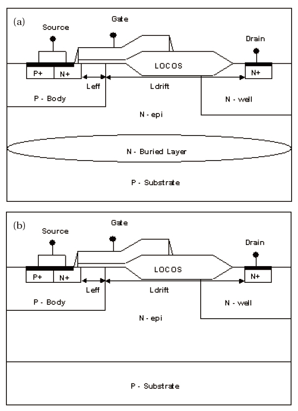
High voltage lateral double diffused metal oxide semiconductor (HV LDMOS) devices are widely used in various applications,such as LCD drivers or RF devices. More recently, HV LDMOS devices have been used in complex analog circuits. Accurately modeling LDMOS transistors for circuit simulation is one of the most important aspects to be considered [1]. The modeling of LDMOS devices is complicated due to the existence of an lightly doped drain (LDD) region and an extended gate region [2]. The BSIM3 SPICE model is widely used as the best model for sub-micron MOS devices, but does not sufficiently model HV devices. In the absence of a suitable physical predictive compatible SPICE model for LDMOS transistors, it was decided to employ a more practical and flexible sub-circuit approach based on the widely used BSIM3 SPICE models [3]. Figure 1 shows the schematic structure of the LDMOS transistors used for 12, 30, 40 and 50 V applications with a gate-oxide thickness (Tox) of 300 ㎕, channel length of 1.8 ㎛ and fabricated with a 0.3 ㎛ CMOS technology.
The two key specifications of LDMOS transistors are a low onresistance (Ron) and a high breakdown voltage (BV). However, these two parameters conflict with each other. For example, increasing the N-well dose not only cause the BV to increase, but also causes the Ron to increase. Device (a), by virtue of the presence of an N-buried layer, has a low Ron and low BV, whereas device (b) has a high Ron and high BV due to the reduced surface field (RESURF) effect.
2.1 Limitations of the conventional SPICE model
2.1.1 Quasi-saturation effect
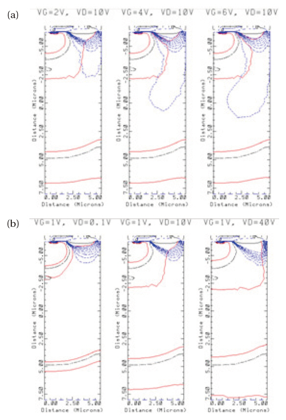
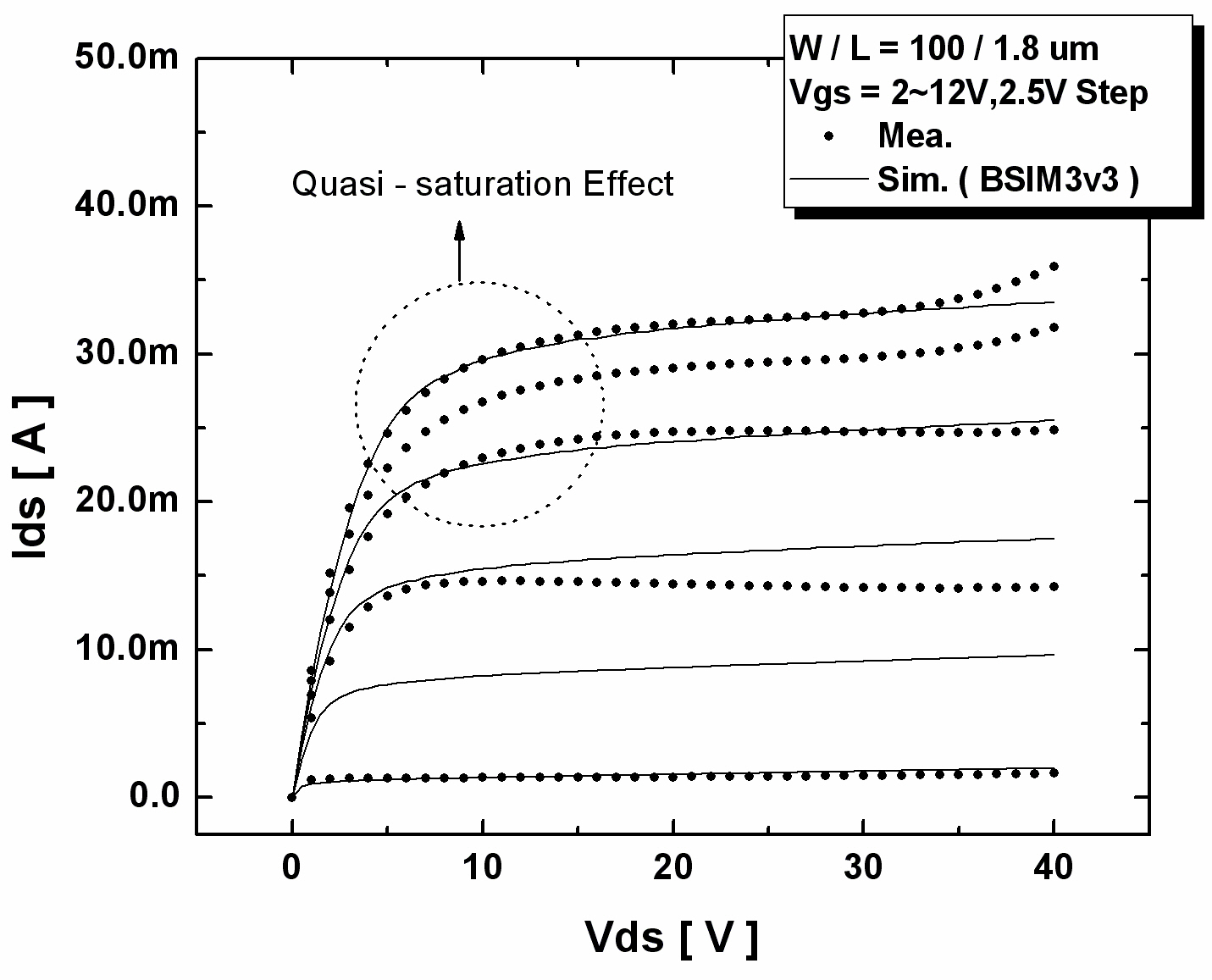
As shown in Fig. 2, the drain current is limited to a certain extent at high gate voltages. This is referred to as the “quasi-saturation effect.” The conventional MOS SPICE model is incapable of modeling this effect, as can also be seen in Fig. 2. Process and device simulations were performed to examine the origin of this effect.
As shown in Fig. 3(a), by increasing Vgs, the depletion regions spread outwards and upwards from P-Body and P-Substrate and, therefore the current flow is confined to the undepleted regions.The flows of current through these regions cause the quasi-saturation effect.
2.1.2 Bias-dependant resistance
Figure 3(b) shows a simulation of the HV LDMOS transistor at a constant Vgs. The drift resistance increases with increasing Vds due to the extension of the depletion region that is formed in the drift region. The current path in the drift regions extends with increasing Vgs at a constant Vds. Therefore, the drift resistance must be a function of Vds and Vgs.
2.1.3 Different Id-Vgs characteristics
In general, the saturation drain current of a metal-oxide semi-
semiconductor field-effect transistor (MOSFET) is modeled by
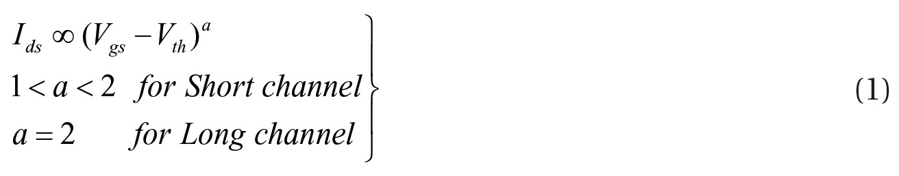
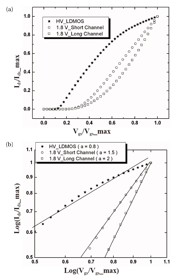
where Vth is the threshold voltage. We can find the value, “a,” viz. the slope of the line, from Fig. 4(b). As shown in Fig. 4(a), while Vgs is greater than Vth, the drain current of a short channel n-MOSFET increases linearly and that of a long channel n-MOSFET increases hyperbolically, whereas the drain current characteristics of an HV LDMOS are different from those of a conventional MOSFET. The conventional SPICE model is sufficient to model 1.8 V CMOS devices, but not for modeling HV LDMOS devices. Because Rdin is a function of only Vgs, as shown in Eq. (2), the drain current of an HV LDMOS device increases complexly (where “a” is about 0.8), as shown in Fig. 2, and consequently the BSIM3 cannot model the quasi-saturation effect and its accuracy is poor. Therefore, we propose a sub-circuit macro model to overcome these limitations.
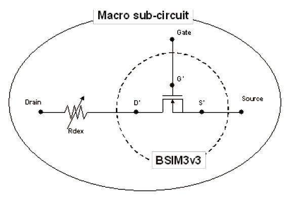
The LDMOS sub-circuit model implemented in this work is shown in Fig. 5. Rdin, as shown in Eq. (2), is the built-in bias dependent resistor model in BSIM3 and Rdex is the bias dependent resistor model of the drift region. We discuss the Rdex in this section.Rdin is modeled by Liu et al. [4].
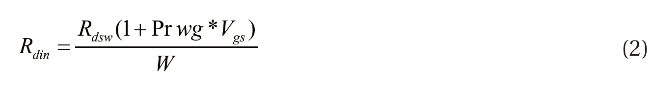
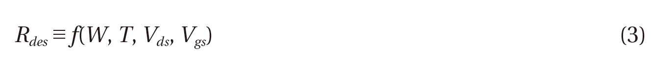
where Rdsw is the parasitic resistance per unit width, W is the channel width, and Prwg is the gate bias effect coefficient of Rdsw. As mentioned above, Rdex can be defined by Eq. (3), because the resistance of the drift region is dependent on Vgs as well as Vds.
We investigated the most appropriate mathematical formulations to describe Rdex. The following continuous mathematical expression is proposed for the drift resistance:
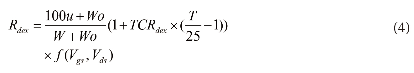
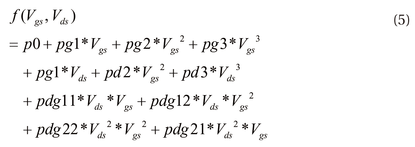
where T is the temperature, Wo is the width offset, pxxx is the bias coefficient for Vgs[Vds] and TCRdex is the temperature coefficient for Rdex.
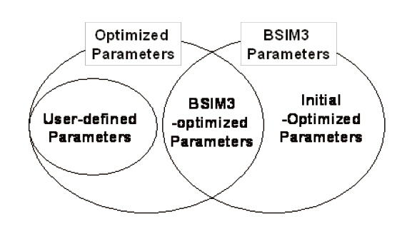
This section describes how to optimize the parameters for the HV LDMOS devices. As shown in Fig. 6, there are three kinds of parameters in our sub-circuit model: the user-defined parameters, BSIM3-optimized parameters and initial-optimized parameters.
First of all, we extracted the initial-optimized parameters with parameter extraction tools such as UTMOST or BSIMProp+ [5],and then optimized the user-defined and BSIM3-optimized parameters. The user-defined and BSIM3-optimized parameters are listed in Table 1. We used the built-in optimizer in the circuit simulator, such as HSPICE or Smart-SPICE, to optimize these parameters. We also used the macro modeling routine in UTMOST. The latter method was more convenient than the former one, because all of the optimization work was performed in a GUI environment.
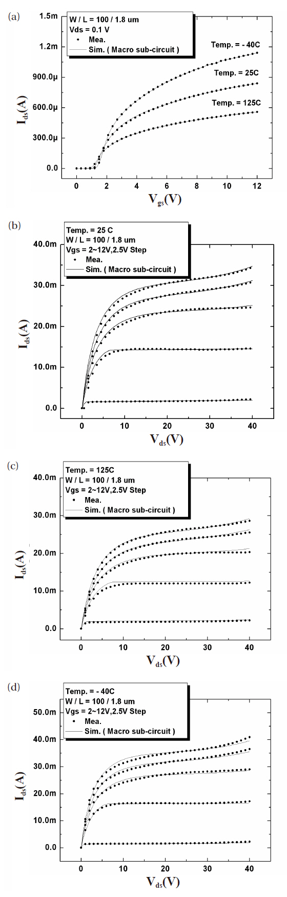
In the previous section, we described various strategies for the optimization of the parameters. The I-V characteristics that were simulated using our macro model with the optimized parameters are shown to validate the sub-circuit macro model. Figure 7 shows that the simulated I-V characteristics are well matched with the measured I-V data.
HV integrated circuits are viable alternatives to discrete circuits in a wide variety of applications. The HV device that is generally used in these circuits is the LDMOS transistor. In this work, we described the electrical characteristics of HV LDMOS devices and the limitations of the conventional SPICE model for
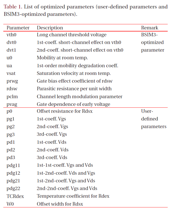
[Table 1.] List of optimized parameters (user-defined parameters and BSIM3-optimized parameters).

List of optimized parameters (user-defined parameters and BSIM3-optimized parameters).
LDMOS devices. Attempts to model LDMOS devices are complicated dues to the existence of the LDD and the extension of the poly-silicon and the gate oxide. Several physically based investigations of the bias-dependent drift resistance of HV devices have been conducted, but a complete physical model has not been reported. The limitations of the conventional SPICE model can be overcome by using a macro model and, consequently, we proposed an accurate LDMOS macro model for circuit simulation.We also present a parameter extraction methodology for the LDMOS macro model. The proposed macro model can be used to obtain accurate circuit simulation results for LDMOS devices.