Organic semiconductors have recently been used as active layers in electronic devices such as field-effect transistors (FETs). In efforts to improve device performance, researchers have allotted great attention to the carrier transport mechanisms of organic semiconductors [1,2]. Copper phthalocyanine (CuPc) materials have exhibited excellent semiconductor performance and have been studied for applications as organic FETs (OFETs).
Material choice changes the work function of an electrode. Furthermore, the surface treatment can control a metal surface’s effective work function. Two surface treatments are the UVozone treatment or the plasma treatment of the substrate and electrode surface [3,4].
For both treatments, the devices studied exhibited operation voltage decreases. This clearly shows that the efficiency of the charge injection from metal to organic layer is strongly dependent on the electronic state at the interface.
The effect of the UV/ozone treatment of the source and drain electrode on the CuPc FET characteristics are studied. Understanding the injection behavior of charges at the metal/organic interface is necessary for improving the FET operation. The transistor characteristics of a top contact CuPc FET are discussed based on the carrier accumulation around the electrode, taking into account the current-voltage (I-V) characteristics.
We were the UV/ozone treatment on the SiO2 layer for the duration of 30 minute. Also, the UV/ozone-treatment carried out with the Au source and drain electrodes before deposited the CuPc material. The UV/ozone-treatment was applied in a UV/ozone-treatment chamber (NL-UV 253S; Nippon Laser & Electronics Laboratory, Tokyo, Japan) filled with oxygen gas. During the UV/ozone-treatment, UV light from a low-pressure mercury lamp was irradiated onto the surface of the SiO2 layer. The CuPc material was purchased from Tokyo Kasei Kogyo Co. Ltd. (Tokyo, Japan) and was used without purification. The CuPc material was deposited through the thermal evaporation method. The CuPc material deposition rate was 0.5 Å/s and. The vacuum level less was maintained at less than 10-6 torr. The substrate was kept at a room temperature.
The samples on the pre-patterned top contact FET substrate and the thickness of the CuPc layer was approximately 40 nm. The deposition rate was monitored by a quartz crystal microbalance (QCM).
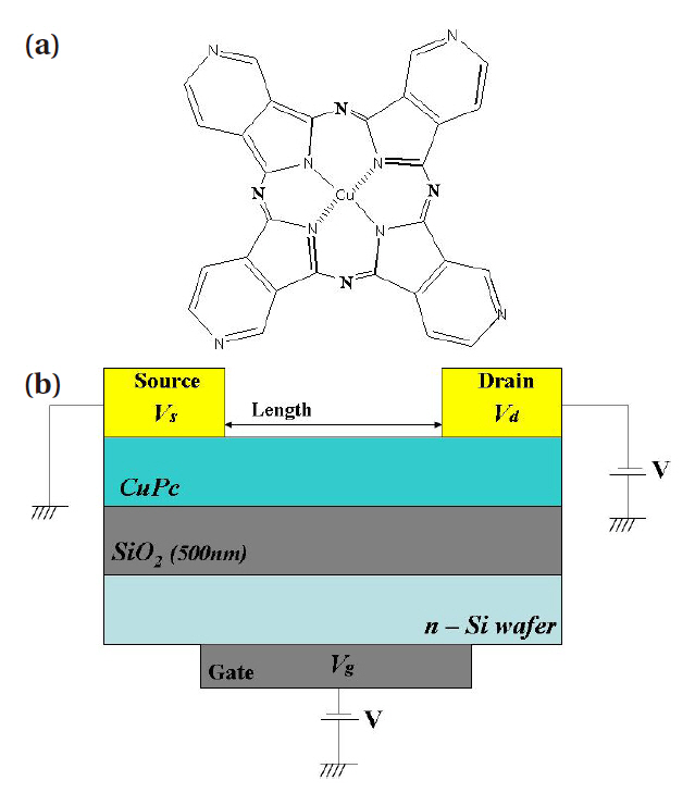
Figure 1 shows a molecular structure and the device structure of the top-contact CuPc FET. The CuPc FET was fabricated using the silicon substrate. The channel length (L) was 100 ㎛ and channel width was 3 mm and also, the active material thickness was about 40 nm. The I-V characteristics were studied under ambient conditions using a source-meter (Keithley type-2400; Keithley Instruments Inc., Cleveland, OH USA).
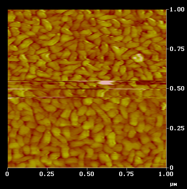
Figure 2 shows the atomic force microscopy (AFM) images of the CuPc thin film surface with the SiO2 substrate. The CuPc materials were layered parallel with the substrate, clearly displaying the CuPc grain.
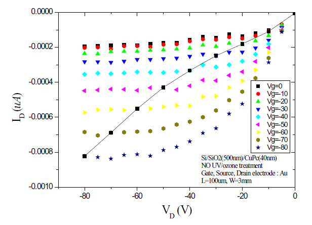
Figure 3 shows the typical I-V characteristics of a CuPc FET using an untreated substrate with the CuPC FET. Gate voltages between 0 and -80 V were applied with a constant scanning rate. Typical FET characteristics were observed though the VD and Vg voltages were very high. VD and Vg represent the applied voltages between drain and source electrodes, and gate and source electrodes, respectively. As shown in Fig. 3, the CuPc FET using an untreated substrate shows enhanced n-channel FET behavior. Interestingly on the other hand, we observed more than faster saturated region of the CuPc FET with a UV/ozone treated sub-
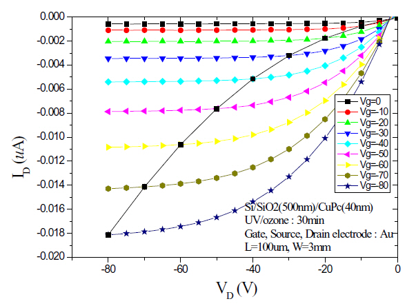
[Fig. 4.] I-V characteristics of the CuPc field-effect transistor with a UV/ozone treated substrate.

strate in Fig. 4.
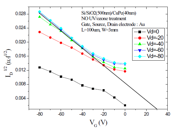
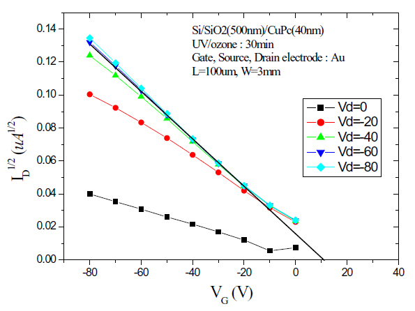
Figure 5 shows the transfer characteristics of the CuPC FET using an untreated substrate. Figure 6 shows the CuPc FET with a UV/ozone treated substrate.
According to the transfer characteristics root( ID -VG) of these FETs shown in Figs. 5 and 6, the threshold voltage, Vth, decreased with a UV/ozone treatment substrate. The threshold voltage was estimated for the UV/ozone-treated and untreated
[Fig. 6.] I-V characteristics of the CuPc field-effect transistor with a UV/ozone treated substrate.

substrate sample about 30 V and 5 V. We also calculated the field-effect mobility of 1.2 × 10⁻⁵ cm2/Vs using the untreated substrate of the CuPc FET device and 1.2 × 10⁻⁴ cm2/Vs with the UV/ozone treated substrate.
Top-contact CuPc FET devices were fabricated. Subsequently,the I-V characteristics of the devices were measured. The I-V characteristics show the similar FET characteristics as the n-type characteristics.
A significant change in the threshold voltage was observed with the UV/ozone treated substrate. The change manifested as a decrease from 30 V to 5 V. We also calculated the field-effect mobility of 1.2 × 10⁻⁵ cm2/Vs an using untreated substrate in the CuPc FET device and 1.2 × 10⁻⁴ cm2/Vs with UV/ozone treated substrate.