An electrically erasable programmable read-only memory (EEPROM) containing a stacked metal-insulator-metal (MIM) and n-well capacitor is proposed. It was fabricated using a 0.18 ㎛ standard complementary metal-oxide semiconductor process. The depletion capacitance of the n-well region was effectively applied without sacrificing the cell-area and control gate coupling ratio. The device performed very similarly to the MIM capacitor cell regardless of the smaller cell area. This is attributed to the high control gate coupling ratio and capacitance. The erase speed of the proposed EEPROM was faster than that of the cell containing the MIM control gate.
During the 1980s, a novel nonvolatile memory product was introduced, referred to as flash electrically erasable programmable read-only memory (EEPROM). The basic operating principle of the nonvolatile memory device is to store charges in the gate oxide of a metal-oxide semiconductor field-effect transistor (MOSFET). If charges can be stored in the oxide of a MOSFET, the threshold voltage of the MOSFET can be modified to switch between two distinct values, conventionally defined as the erase state and the program state. The terms erase and program are used to denote operations that charge and discharge through oxide. The threshold voltage shift between the two states is caused by the storage of charge in oxide. The program state is usually obtained from a channel hot electron, while the erase state uses Fowler-Nordheim (F-N) tunneling through a thin gate oxide. The storage of charges in the gate oxide of the nonvolatile memory device can be realized by surrounding a conducting layer by an oxide. Since this layer acts as a completely electrically isolated gate, this type of device is commonly referred to as a floating gate device.
An EEPROM cell containing an n-well and metal-insulatormetal (MIM) capacitor was fabricated using a 0.18 ㎛ standard complementary MOS (CMOS) process. In recent efforts, a stacked metal-insulator-metal (MIM) and an n-well capacitor have been applied to a single polysilicon EEPROM cell in order to increase memory capacity [1-4]. The application of the single polysilicon EEPROM is becoming more popular due to its low process cost and satisfactory reliability [5-7]. Optimal characteristics of EEPROM include fast program/erase speed, high endurance performance, and low leakage current. Although the MIM capacitor cell performs well, it requires a large device-size. The n-well control gate cell inherently possesses high junction capacitance and high sheet resistance.
In this paper, we propose an EEPROM cell that does not require additional cell area in order to obtain a high capacitance.Additionally, the proposed EEPROM provided a satisfactory control gate coupling ratio contributing to the junction capacitance between the control gate and the n-well. Because the n-well depletion capacitor was isolated by shallow trench isolation (STI) and the MIM capacitor was located just above the n-well capacitor, the cell containing two capacitors connected in parallel was expected to be very reliable and to provide noise immunity.
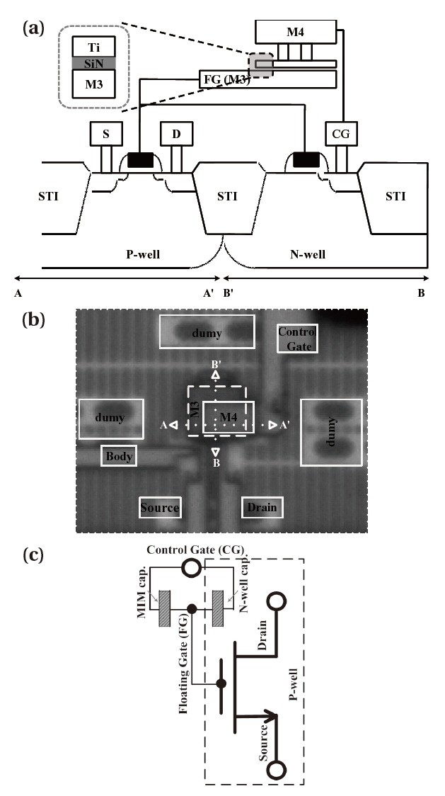
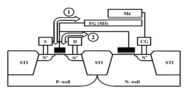
EEPROM cell technology falls into two basic cell structures:planar and non-planar. The difference between the two structures is that, in the planar, the electron injection field is equal to the average tunnel oxide field, while in the non-planar structure, the average tunnel oxide field is much smaller than the injection field. The program operation transports electrons to the floating gate in our planar cell structure, while the erase operation removes electrons from the floating gate. Fig. 1 is the schematic of the proposed device. The EEPROM cell contains an n-channel MOSFET, a floating gate, n-well capacitor and MIM capacitor. The MIM capacitor is composed of metal (M)-3, intermediate plasma-enhanced chemical vapor deposition SiN, Ti and metal- (M)4. The thicknesses of the Ti and SiN layers are 1,200 Å and 800 Å respectively
In the equivalent circuit in Fig. 1(c), the two MIM and n-well capacitors are connected in parallel between the control and floating gate. The floating gate was an M3 layer in the MIM capacitor which was also connected to the polysilicon gate of the n-well capacitor. The control gate was connected through N+ region in n-well and M4. The calculated coupling ratio of the cell was 0.67.
A 0.18 ㎛ standard CMOS logic process was used to fabricate the EEPROM cell. The thickness of the tunnel oxide was 37 Å. STI, twin-well, poly-Si gate, n-lightly doped drain (LDD) ion implantation (I/I), LDD spacer, source/drain (S/D) I/I, TiSi2 formation contact, Ti, and six-level metal interconnections were carried out sequentially.
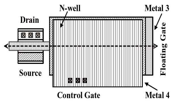
The illustration of the alignment in Fig. 2 is designed so that control and floating gates connect the two capacitors through M4 and M3 in parallel.
The erase operation of the EEPROM cell is comprised of a certain procedure. Before the cell was programmed, no charged exist on the floating gate and the device operated as a regular n MOSFET. The erase operation was done with a high Vs (source voltage) of 5.5 V and a low Vcg (control gate voltage). Fig. 3 shows the path of the charge transport in the capacitors of the MIM and n-well. During the erase operation, electrons in the MIM and n-well capacitors were distributed to source (s) through the path of 1 and 2. The circuit was designed so that the capacitances of MIM and n-well were equivalent. Additionally, the control gate coupling ratios also designed to be equivalent. In our cell, the two separate capacitors speed up the erase operation. Note that the size of our cell is almost half the size of the MIM capacitor cell and the coupling ratio (αCG) of the cells did not decrease during the erase operation.
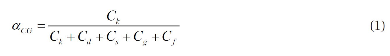
The control gate coupling factor (αCG) is given as the ratio of capacitances, where Ck is the total capacitance between the floating gate and control gate. Equation (1) is the control gate coupling factor (αCG), where Cs, Cd, Cg, and Cf are the source, the drain, the floating gate channel, and the field region capacitances, respectively. Two important coupling ratios are the control gate coupling factor and the drain-coupling factor.
The effective capacitance ratios determine the fraction of the control gate and the drain voltage. A capacitance that is often omitted in determining the coupling factors is the coupling capacitor between floating gate and substrate through the field oxide. In the EEPROM cell, this capacitor is important because of the large coupling area between the floating gate and the control gate located over the field oxide.
The capacitor values are estimated by using a simple parallelplate model. However, fringing capacitances should also be taken into account. In thin oxide, normally the parallel-plate approximation is fairly good, and the fringing effects cause a deviation of only a few percentage.
Usually, Ck and Cg are larger than the other capacitances. Taking account of these two factors enables us to simplify the expression for αCG to Eq. (2).
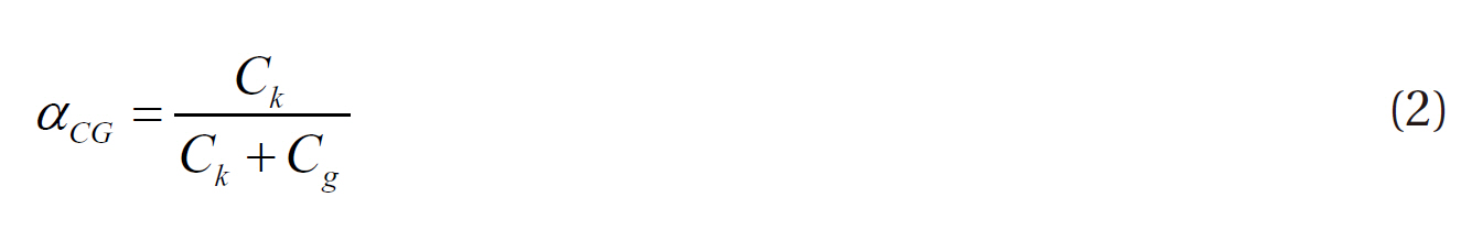
This expression indicates that the larger Ck increases the αCG.The capacitance between the floating and control gate, Ck, is the dominant factor in determining the control gate coupling ratio.
In the program operation using Vcg of 5 V and VDS of 3.5 V, the proposed EEPROM cell induces a channel hot electron and delivers the hot electron to the floating gate by the high control gate voltage similar in procedure as the conventional EEPROM. The channel hot electron can be achieved by applying a high voltage to both the drain and control gates simultaneously. With the control gate high, the high voltage across the drain to source gives a high channel current and channel field which generates hot electrons. The high voltage on the control gate couples a voltage to the floating gate and attracts hot electrons to the floating gate. Instead of programming the drain side by channel hot electron, it is possible to design an EEPROM cell that makes use of a narrow gap produced by a poly spacer on the source side in order to obtain a local high field for programming. In the erase operation, F-N tunneling is used from the floating gate to source. F-N tunneling current is generally a strong function of the electric field and occurs in SiO2. The erase operation is obtained with the application of high voltage in the source. Another erase operation can be possible by applying a negative voltage to the control gate. The source can either be grounded or kept at a lower voltage. However, a switching of negative voltage increases circuit complexity.
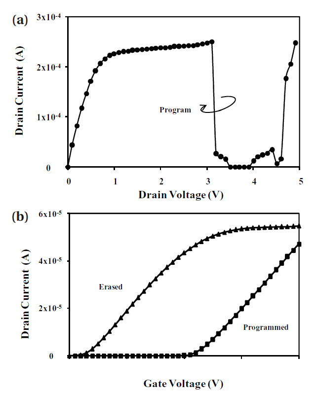
In this experiment, the area of the MIM capacitor in the proposed cell was reduced that the size of the MIM cell and another half capacitance was supplied from n-well capacitor. The electrical characteristics of the MIM capacitor cell and our proposed cell which possessed MIM and n-well capacitors were compared in terms of drain current versus drain voltage and control-gate voltage. The current-voltage characteristic was similar to that of a regular n-MOSFET.
Figure 4(a) shows the one-shot programming characteristics of our proposed cell at a control gate voltage (VCG) of 3V. Starting from zero current, if the drain voltage increased, the drain current also increased. but, the rate of rise fell until the drain current eventually reached a constant value. The saturation region is the area where the drain current is no longer affected by the drain voltage, and where the device acts more like a current source. As drain voltage increased, the saturation region became elevated after the triode region. The dividing line between triode and saturation regions is where the voltage drop across the gate oxide falls below threshold voltage, causing the channel to pinch off. Sharp decreases of the drain current in the saturation region signified that hot electrons in the channel moved toward the floating gate (M3), indicating the program state. With a small floating gate capacitance, achieving an ef-
efficient program was not possible. The change of drain current was dependent on the size of capacitor in the floating gate. The drain current at the saturation region reached 0.24 mA. Even though the proposed cell contained a LDD S/D junction, the channel hot electron program occurred at a drain voltage of about 3.1 V, which is almost the same as the MIM cell. The erase and program threshold voltage can be written as the Eqs. of (3) and (4).
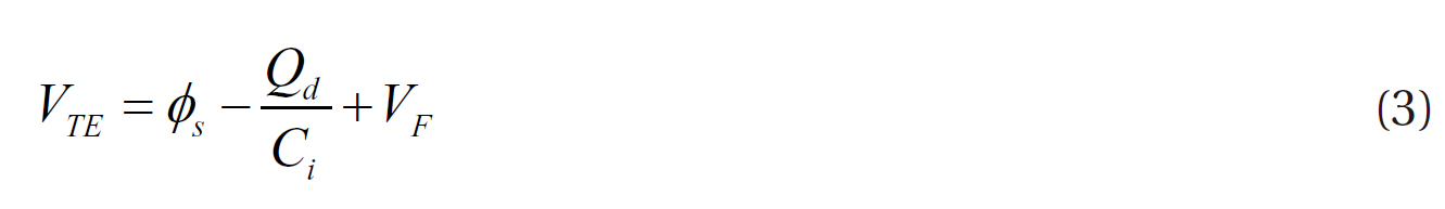
where VTE, Qd, Ci, and VF are erase threshold voltage, surface potential, charge in depletion region, and flat band voltage, respectively
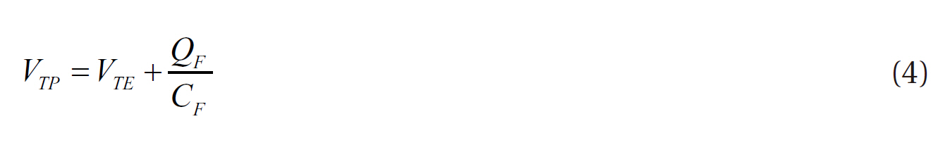
In the program threshold voltage VTP, QF and CF are the charges in floating gate and capacitance from floating gate, respectively. The two threshold voltages were almost independent of the capacitor size and the difference between the two threshold voltages depended on the charge in the floating gate.
In the characteristic of the drain current versus gate voltage (ID-VGS) of Fig. 4 (b), the program and erase threshold voltages were 2.2 and 0.5 V, respectively. The difference between the program and erase threshold voltages originates from the charge in the capacitor between the floating gate and control gate.
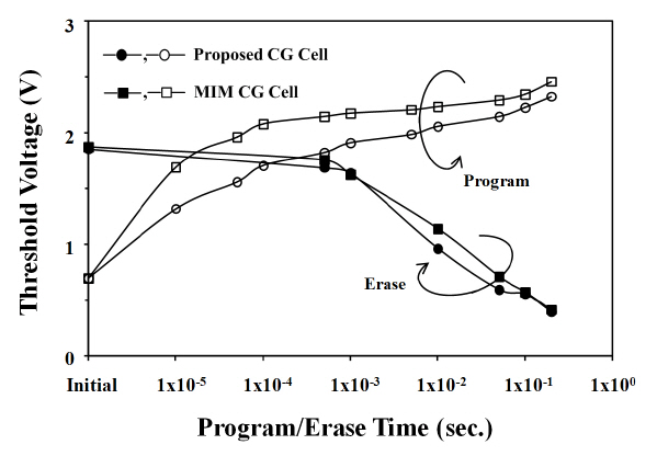
Figure 5 shows that the program and erase characteristics the MIM capacitor cell and our proposed cell. Calculated from the layout dimensions and process parameters, the control gate coupling ratio (αCG) of the two cells was adjusted to 0.67. In order to achieve an acceptable capacitive coupling ratio between the floating gate and the word-line, the area of the floating gate was made much larger than the minimum lithography limits.
This improved redundancy and error correction. From an initial to program/erase time of 0.2 s seconds in the F-N tunneling erase characteristics, the erase speed of the proposed EEPROM was faster than that of the cell with MIM control gate. Junction depletion occurred on top of the source LDD region during the erase process because the floating gate potential was lower than the source LDD junction potential. In our cell, the split charge transport operation resulted in a faster erase operation. The proposed EEPROM cell was smaller than the MIM capacitor cell and the coupling ratio (αCG) of the cells did not decrease during the erase. In the program characteristic based on the hot electron effect in the channel, the proposed EEPROM cell exhibited a slower programming speed and less threshold voltage shifts compared to the cell of the MIM control gate. This is due to the lower effective αCG caused by the depletion and junction capacitance of the n-well. The effective αCG of our cell reduced to 0.60 from the initially designed value of 0.67.
EEPROM was dependent on the integrity of the memory device dielectrics for reliable device performance. Failure in the gate oxide and capacitor contributed to both retention and endurance failure. In addition, since EEPROM operated similarly to the MOS integrated device, it suffered reliability failures in a similar fashion as the MOS device. Because of the high electric field needed to write and erase the EEPROM device, higher than typical MOS circuit voltages were usually routed through some of the MOS circuit elements. Therefore, the EEPROM device was expected to experience higher electric field stress under normal operating conditions. The device would exhibit higher failure rates if the design was not properly executed with careful considerations taken during the fabrication process, device structure,and circuit realization. The repeated transport of charges across the thin oxide resulted in memory cell degradation, which in turn produced a limit for the program/erase cycle.
Endurance is defined by the number of data changes that can be performed on every cell of EEPROM device before one of its cells fails to meet its data specification, while retention can be quantified by measuring or estimating the time it takes for the floating gate capacitor to discharge when it is intended to keep
the information stored. Endurance describes the reliability of the EEPROM in terms of program/erase operations that can be performed on it without failure.
After transient time, the stable program and erase threshold voltages were measured as 2.4 V and 0.3 V respectively. During the endurance characteristics tests which lasted 5 × 10⁴ program/erase cycles, we found that the shift of the threshold voltage was negligible and the drain current was almost constant. Charge injection through oxide whether by F-N tunneling or hot carrier injection caused degradation due to broken bonds and charge trapping, eventually leading to breakdown.
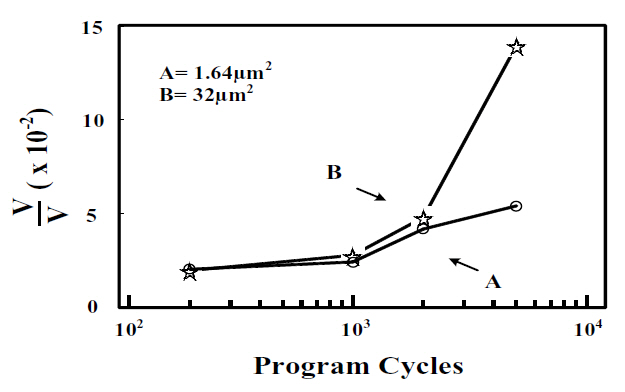
With an increase in the size of the MIM capacitor, the data retention and endurance of program characteristic deteriorated. Figure 6 shows the shift of the program threshold voltage after the program/erase cycles. The shift of threshold voltage was attributed the hot electron effect and gate oxide degradation. Impact ionization created hot electrons and holes. The experimental result was obtained with two different capacitor areas, indicating that the shift of the program threshold voltage increased with the increase of the area in MIM capacitor cell.
In particular, after 2 × 10³ W/E cycles, the voltage shift drastically increased for the small MIM capacitor. Up to 2,000 cycles, the shift of threshold voltage was within 5%. The voltage shift was attributed to the oxide degradation and trapped charges in the channel. The holes accumulated at the substrate and raised the potential, while electrons were trapped in the oxide. The substrate potential increased the substrate current, which itself was related to the amount of hot electrons generated. The increase of substrate potential will, in turn, decrease the program threshold voltage.
Charge and traps in SiO2 have been studied extensively because of their technological importance in MOS technology. The primary degradation mechanism of the oxide pertains to dielectric breakdown due to high field/current stress, modifying the physical properties dominated by the traps, and trapped charge in oxide. Breakdown due to oxide degradation and extrinsic defects can be viewed as time-dependent breakdown (TDDB). The accidental deformations can give rise to material constants and geometric parameters that result in reduced times to failure. The large size of MIM capacitor can be suggested for a high speed EEPROM and good memory capacity, device reliability is not good as much as that of thin oxide cell.
An EEPROM cell containing n-well and MIM capacitors was proposed. The cell fabrication was completed using the 0.18 um standard CMOS process. The control gate was connected through N+ region in N-well and M4. With the implication of the n-well depletion capacitor to MIM capacitor, the cell size can be significantly reduced. Even with a smaller cell area, the device performed exceptionally similarly to the MIM capacitor cell. The endurance characteristics of the cell up to 50,000 cycles were demonstrated. The threshold voltage windows were 1.7 V after 10,000 cycles without degradation of the read current. The shift of the program threshold voltage can be significantly dependent on the size of the MIM capacitor.