This study has been carried out to determine the optimal process conditions of AZO:H2 thin films for the maximization of the transmittance of a blue GaN light-emitting diode (LED) with a wavelength of 470 nm. The Al-doped zinc oxide (AZO):H2 thin films were deposited on a sapphire substrate by radio-frequency magnetron sputtering system with varying substrate temperatures, working pressures and annealing temperatures temperature, working pressure and annealing imposed on a AZO (2wt% Al2O3) ceramic target. The effect of these variables was investigated in order to improve the light extraction efficiency of the LED. As a result, the (002)-oriented peak was found in all the AZO:H2 thin films. The lowest resistivity and the best transmittance at a wavelength of 470 nm was found to be 4.774 × 10⁻⁴ Ωcm and 92% at a substrate temperature of 500℃, working pressure of 7 mTorr and annealing temperature of 400℃. The transmittance of the AZO:H2 thin film for the Blue GaN LED was improved by approximately 13% relative to that of a ITO thin film (T = 79%).
Recently light-emitting diodes (LEDs) have been widely applied for use in a variety of optoelectronic devices such as LCD back light unit, mobile phone displays, signal lamps, automobile and illumination display panels and so on. Normally, a blue GaN LED and fluorescent material (YAG) are used to make a white LED, as the blue GaN LED has the larger energy. Especially, the blue GaN LEDs are attractive due to their high brightness and high power capability in lighting and display applications. The internal quantum efficiency of a Blue GaN LED has been developed to an almost optimum stage.
However, the critical angle is 23.5°, as a consequence of the refractive indexes of GaN (n = 2.5 at 470 nm) and air. Only about 4% of the emitted light radiates through the top and bottom [1]. There are many technologies such as a transparent electrode,a die shaping technology, a wafer bonding technology and an epoxy dome technology and so on for improving the light extraction efficiency of a blue GaN LED with a wavelength of 470 nm.This paper reports on the adoption of a transparent electrode to improve the light extraction efficiency of this LED, and the electrode being used to match refractive index between GaN and air.
Al-doped zinc oxide (AZO) holds advantages in the respects of low cost, being free of toxic materials and stability against hydrogen plasma. Especially, It has a much higher transmittance than that of indium tin oxide (ITO, T = 79%) for the blue GaN LED under investigation. Due to these factors, the AZO film has been considered to be the most potentially viable alternative to ITO,
[Table 1.] Deposition conditions of AZO:H2 thin films by RF magnetron sputtering and annealing.
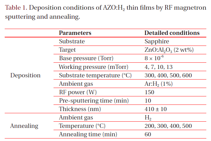
Deposition conditions of AZO:H2 thin films by RF magnetron sputtering and annealing.
which has already been extensively adopted as a transparent conducting film material, but is becoming extremely expensive because of the rare metal indium is becoming in increasingly short supply and also it has a low transmittance due to a high absorption ratio at the wavelength of 470 nm [2].
Under the various growth conditions such as work pressure,substrate temperature and annealing temperature, the growth of ZnO-based thin films has been widely investigated [3]. However, studies on light extraction efficiency for the blue GaN LED with a wavelength of 470 nm using AZO-based thin film are rarely found in t published literature.
In this paper, a study on the optimal process conditions for aAZO:H2 thin film was investigated to improve light extraction efficiency of the blue GaN LED of interest, by the use of an radiofrequency (RF) magnetron sputtering system.
The AZO:H2 thin films were deposited on a sapphire substrate by an RF magnetron sputtering system with a base pressure of 8 × 10⁻⁶Torr using a AZO (2wt% Al2O3) ceramic target [4,5]. The substrates were ultrasonically cleaned sequentially in acetone, alcohol and de-ionized water and dried with nitrogen gas. The
H2/(Ar+H2) percentage was maintained at 1% [6]. The working pressure was varied from 4 to 13 mTorr. The substrate temperature was changed from 300 to 600℃. The AZO target was presputtered for 10 minutes to remove surface contamination and maintain the system stability. The thickness of the AZO:H2 films was 410 ± 10 nm [7]. The distance between the target and the substrate and the RF power were 60 mm and 150 W, respectively[8]. The annealing treatments were carried out by changing the annealing temperature from 200℃ to 500℃ in hydrogen ambient for 60 minutes [6].
The phase and crystal structure of the deposited AZO:H2 films were determined by X-ray diffraction (XRD: Riraku, Max 2500H; Japan). The film thickness and surface morphology were examined by field emission scanning electron microscopy (FE-SEM:Hitachi, S-4800; Japan). The optical transmittance of the films was measured by a UV-Vis spectrophotometer (Scinco, S-3100; Korea) in the wavelength range of 350-1, 100 nm. The electrical properties were examined by the Hall effect system (Ecopia,HMS-3000; Korea) using Van der Pauw geometry. The details of the deposition and annealing conditions of the AZO:H2 thin films are listed in Table 1.
3.1 The micro-structural properties
3.1.1 The working pressure
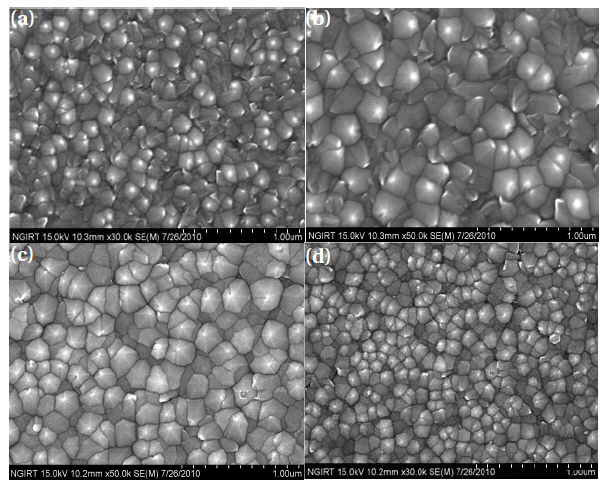
Figure 1 shows the surface morphologies of the AZO:H2 thin films prepared at a working pressure which was varied from 4 to 13 mTorr. The figure shows that the grain size of the AZO:H2 thin films deposited at various working pressures is quite different. The higher working pressure may result in a lower growth rate, smaller grain sizes and with inferior crystallinity.
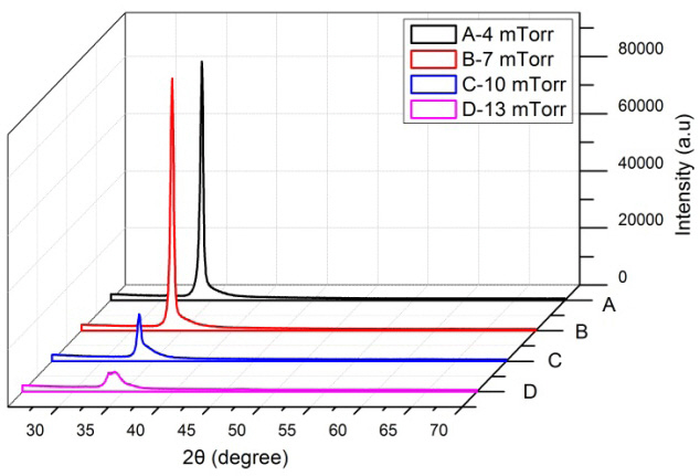
Figure 2 demonstrates the XRD patterns of the AZO:H2 thin films deposited under various working pressures. All of the AZO:H2 thin films show the dominant two theta (002) diffraction peak with the crystal c-axis perpendicular to the substrate in XRD patterns. The (002) peak of the AZO:H2 thin film deposited in an Ar:H2 ambient atmosphere is situated at 2θ = 34.3°, which is close to that of the standard ZnO (34.4°). At low working pressure, the (002) diffraction peak is extremely strong. The working pressure demonstrates a noticeable effect on the microstructure of the AZO:H2 thin films considered in this study. The sputtered materials possess a mean free path that is comparable to the distance from the target to substrate at a lower working pressure. These starting materials have a much higher activation energy
that results in a higher surface mobility and thus a much greater possibility of forming AZO:H2 thin films [9].
3.1.2 The substrate temperature
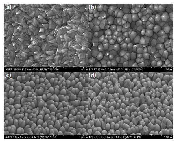
Figure 3 shows the FE-SEM images of AZO:H2 thin films deposited at different substrate temperatures. The grain size increased as the substrate temperature increased from 300 to 500℃. This result invites speculation that the microstructure would be strongly related to the substrate temperature during the deposition.
Figure 4 shows the XRD patterns of the AZO:H2 thin films deposited at various substrate temperatures. All of the AZO:H2 thin films show a c-axis preferred orientation without any detectable secondary phase of Zn, Al and Al2O3. The intensity of the (002) diffraction peak increased as the substrate temperature increased from 300 to 500℃. This result It demonstrated that the AZO:H2 thin film was crystallized or that the growth of crystallinity was accelerated due to the diffusion of sputtered atoms in to substrate, an effect that would increase with increasing substrate temperature. The decrease of the diffraction peak at 600℃ demonstrates the re-evaporation of the deposited particles as a result of an excessive increase in substrate temperature.
3.1.3 The annealing temperature
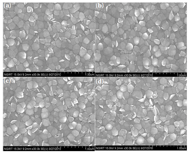
Figure 5 shows the grain sizes of the hydrogen-annealed films
with various annealing temperatures. The grain size changed with annealing temperature. The grain sizes of the AZO:H2 thin films changed from 110.21 to 132.7, 146.32 and 140.81 nm respectively as the annealing temperature increased from 200 to 400℃.
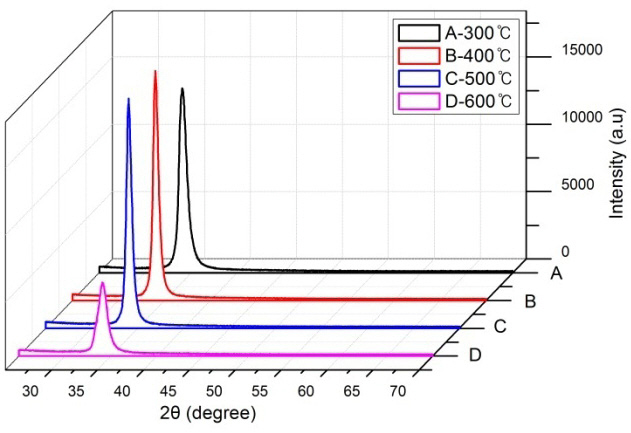
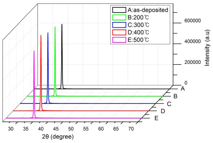
Figure 6 demonstrates the XRD patterns of the AZO:H2 thin films annealed at various temperatures between 200℃ to 500℃.All of the AZO:H2 thin films show the dominant two theta (002) diffraction peak with the crystal c-axis perpendicular to the substrate in the XRD patterns.
The (002) peak of the AZO:H2 thin film deposited in an Ar:H2 ambient atmosphere is situated at 2θ = 34.216°, which is smaller than that arising with the standard ZnO. This result implies that the crystal c-axis of the film grown in the hydrogen-mixed gas was prolonged.
In order to examine the characteristics of the AZO:H2 film, the crystallite extent was estimated. The FWHM values for the AZO:H2 films decreased from 0.075 to 0.058 as the annealing temperature increased from 200 to 400℃.
It was observed that the crystallinity improved with increasing annealing temperature, since the (002) diffraction peak became more intense and sharper. This result indicates that the grain size became larger with increasing annealing temperature. The FWHM and the intensity of the XRD peak increased with temper-
ature and then subsequently decreased at temperatures around or higher than 500℃. The grain size was estimated by use of the Scherrer equation. The Debye-Scherrer’s equation is given by
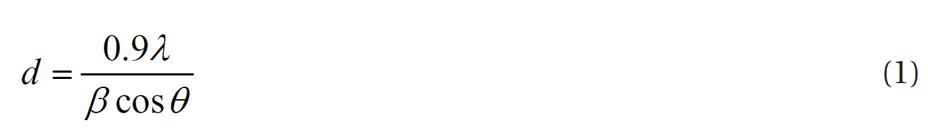
where d is crystallite size, λ is the wavelength of X-ray, θ is Bragg diffraction angle and β is the full width at half maximum (FWHM).
3.2.1 The working pressure
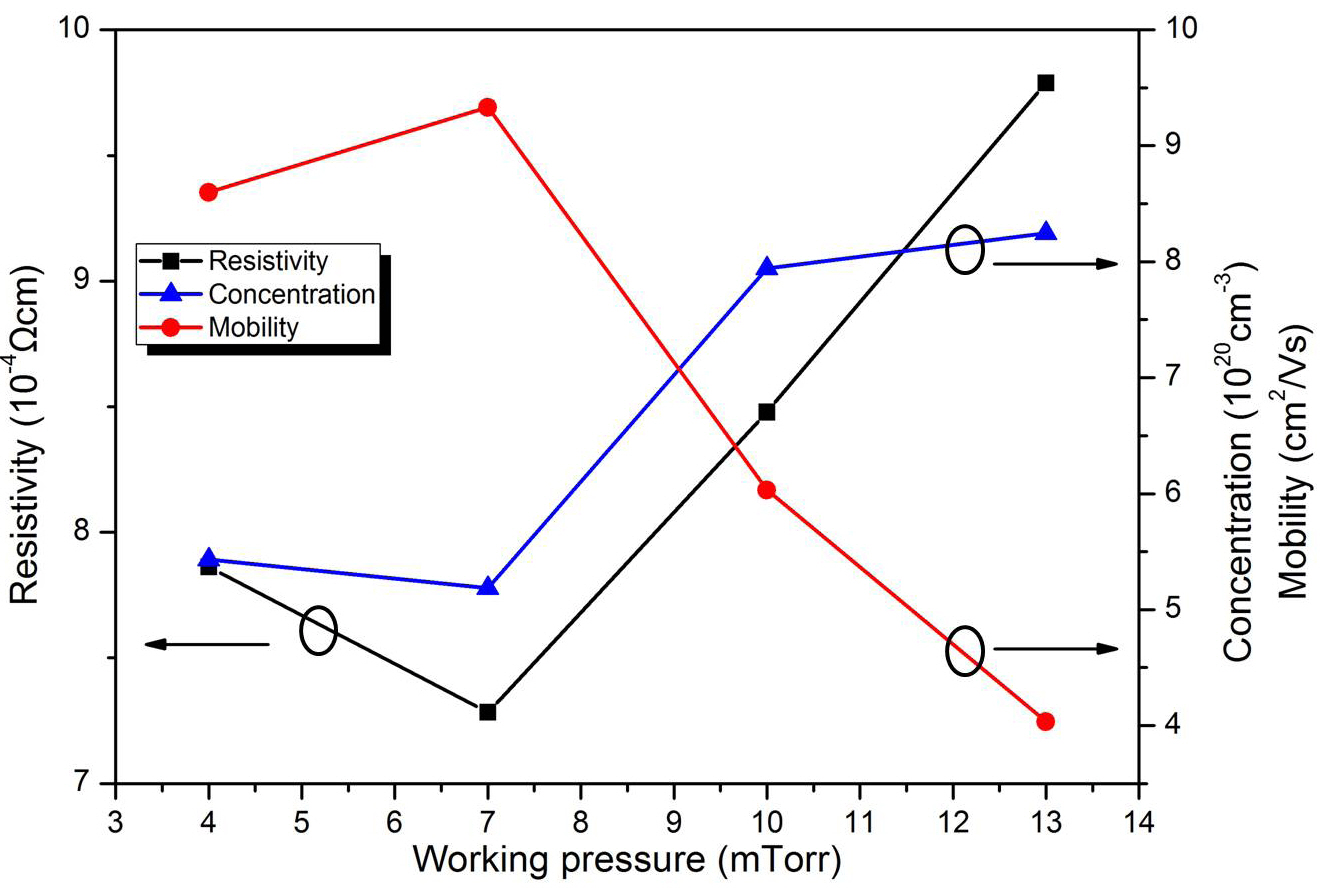
Figure 7 shows the influence of the working pressure on the electrical resistivity of the AZO:H2 thin film. It can be observed that the resistivity increased from 7.283 × 10⁻⁴ Ωcm to 9.788 × 10⁻⁴ Ωcm as the working pressure is increased from 7 to 13 mTorr. The electrical resistivity is well known to be proportional to the reciprocal of the product of the change in carrier concentration and mobility. This effect demonstrates that the energy of sputtered particles was increased as a mean free path of the sputtered particle was prolonged and therefore the crystallinity of the AZO:H2 thin film was promoted.
3.2.2 The substrate temperature
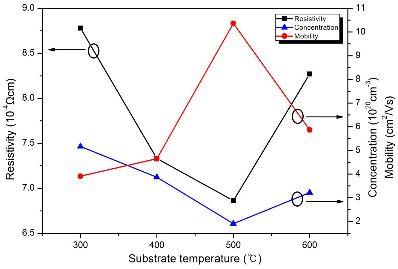
Figure 8 shows the influence of various substrate temperatures on the electrical properties of the AZO:H2 thin films. The resistivity decreased from 8.78. × 10-4 Ωcm to 6.863 × 10⁻⁴ Ωcm as the substrate temperature was increased from 300 to 500℃ because of the evolution of the micro-structure. At 600℃, the resistivity increased to 8.27 × 10⁻⁴ Ωcm. The increase in mobility due to the substrate temperature should influence dominantly the decrease in the resistivity. Lin et al. reported that the change in the resistivity was mainly caused by the change in the mobility in the AZO:H2 thin films [10].
3.2.3 The annealing temperature
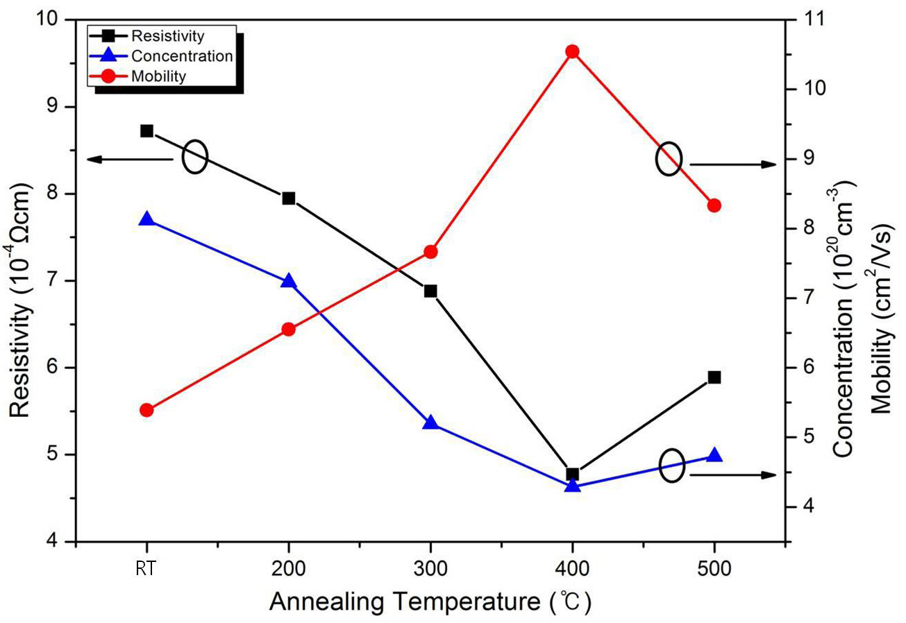
Figure 9 shows the influence of the annealing temperature on the electrical properties of the AZO:H2 thin films After H2 annealing,the resistivity decreased from 8.721 × 10⁻⁴ Ωcm to 4.774 × 10⁻⁴Ωcm as the annealing temperature increased from 200 to 400℃.The improvement in theelectrical conductivity of the AZO:H2 films may be ascribed to the function of oxygen vacancies. According to Wang, annealing in a hydrogen atmosphere may lead to oxygen annihilation and the formation of oxygen vacancies in the lattice [11]. In our experiments, the AZO:H2 films were annealed in a hydrogen atmosphere. It is found that the hydrogen
annealing treatment would be helpful for the promotion of the desorption of oxygen in the grain boundaries which act as traps for the carriers [12]. This may be an another factor that improves the electrical conductivity of the AZO:H2 films.
3.3.1 The working pressure
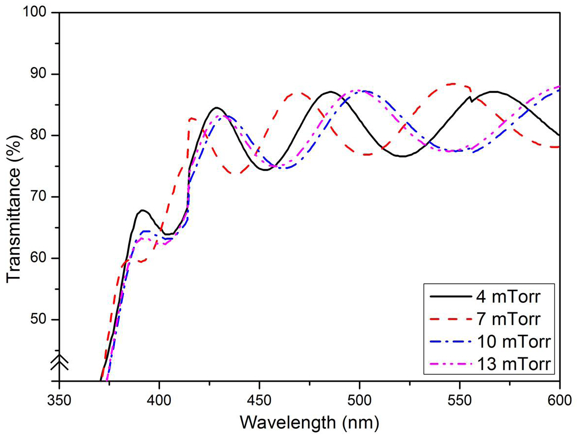
Figure 10 demonstrates the optical transmission spectra of AZO:H2 thin films as a function of wavelength prepared at various working pressures. The best optical transmittance in the wavelength of 470 nm is 87% at 7 mTorr. This is an 11.2% improvement on the transmittance of AZO:H2 thin film deposited at 13 mTorr (T = 75.8%). At higher working pressures, the composition of the AZO:H2 thin films becomes highly nonstoichiometric[9].
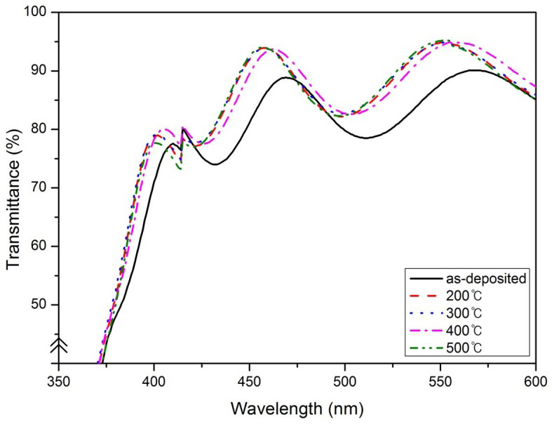
3.3.2 The substrate temperature
Figure 11 shows the transmission spectra of the AZO:H2 films prepared with various substrate temperatures. The best optical transmittance at the wavelength of 470 nm is 86.7% at 500℃.
This result is a 10.9% improvement on the transmittance of a AZO:H2 thin film deposited at 400℃ (T = 75.8%). The absorption edge was shifted to the short wavelength (blue shift) as the substrate temperature increased from 300 to 500℃. This is the Burstein-Moss (BM) effect [13]. The result suggests that the light transmittance was improved because of the growth of particles and an improvement in crystallinity.
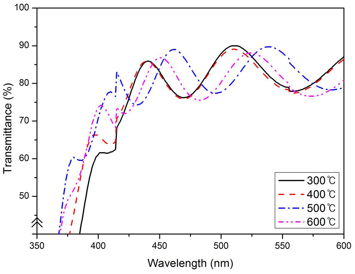
3.3.3 The annealing temperature
Figure 12 shows the transmission spectra of the AZO:H2 films prepared with different annealing temperatures. After H2 annealing,the best transmittance at wavelengths around 470 nm is 92.3% at 400℃, which is a 3.5% improvement on the transmittance of a AZO:H2 thin film deposited at 7 mTorr and 500℃ (T =88.8%).
The change in the optical band gap of the Al-doped ZnO films is mainly affected by two competing phenomena. One is the BM band-filling effect, which leads to a widening (blue shift) of the band gap with increasing carrier concentration. The other is a many-body effect such as the exchange energy due to electronelectron and electron-impurity interactions, which leads to a narrowing (red shift) of the band gap when the electron concentration exceeds the Mott critical value [3]. In our experiment, it was found that the absorption edge shifted to the short wavelength(blue shift) after annealing.
The cut-off behavior at the end of the optical absorption spectrum is determined by direct electronic transition from the valence band to the conduction band.
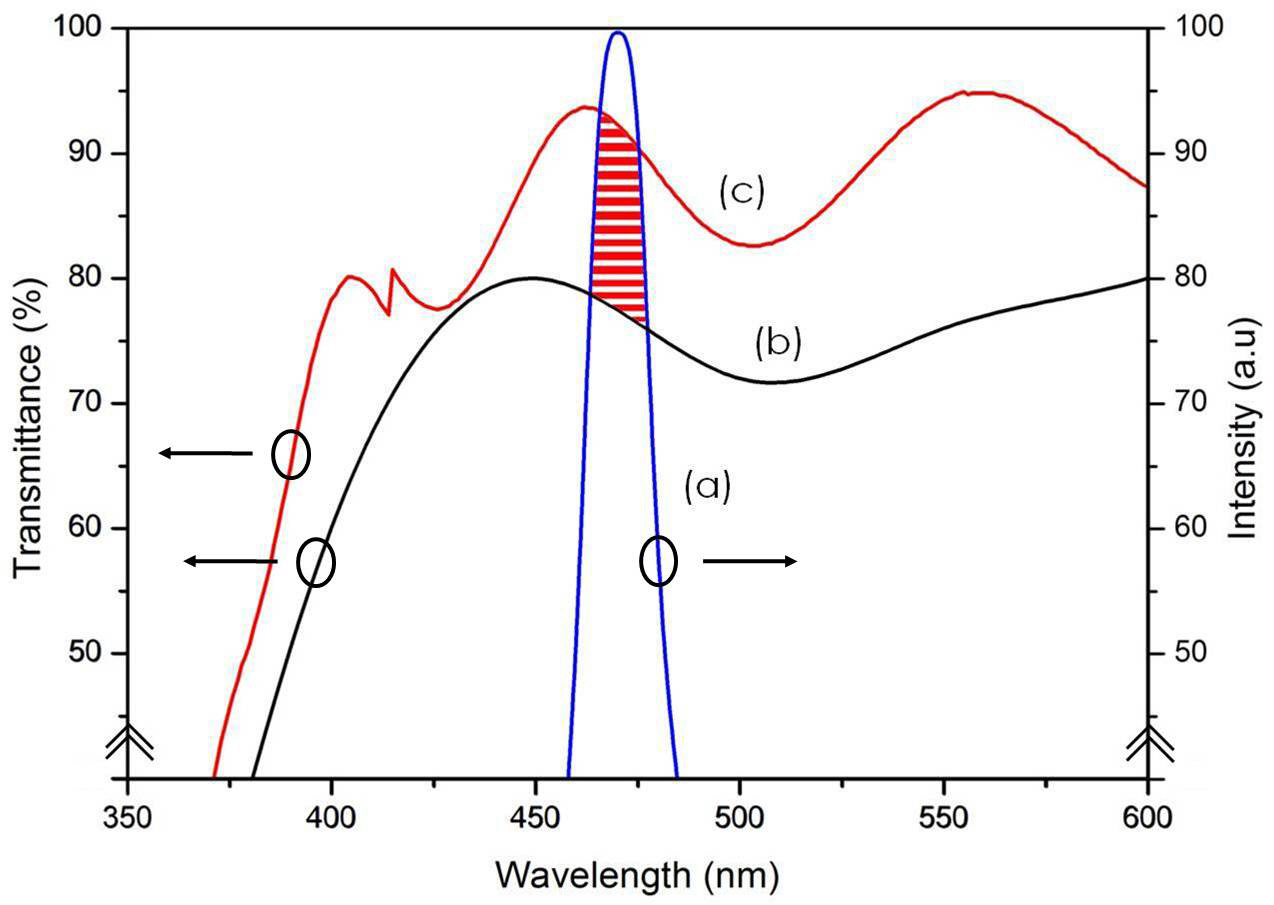
Figure 13 illustrates the spectra of (a) GaN LED [14], (b) ITO thin film [15] and (c) AZO:H2 thin film. The AZO:H2 thin film deposited at a working pressure of 7 mTorr and substrate temperature of 500℃ was annealed at 400℃. The transmission of AZO:H2 is 92.3% in a wavelength of 470 nm. This is much higher than that of ITO (T = 79%), suggesting that the use of the AZO:H2 thin film can improve the light extraction efficiency for a GaN LED and it is suitable for this intended application.
This study has been intended to determine the optimal process conditions for a AZO:H2 thin film for maximization of the transmittance of the Blue GaN LED with the wavelength of 470 nm. The AZO:H2 thin films were fabricated through an RF magnetron sputtering system using a AZO (2 wt% Al2O3) ceramic target. The optimal process conditions were found to be a substrate temperature of 500℃ (T = 86.7%), a working pressure of 7 mTorr(T = 87%) and an annealing temperature of 400℃ (T = 92.3%). The resistivity and transmittance at the optimal process conditions of the AZO:H2 thin film are 4.774 × 10⁻⁴ Ωcm and 92% at the wavelength of 470 nm. This result showed that the transmittance of the AZO:H2 thin film was improved by approximately 13%compared with an ITO thin film (T = 79%) at the wavelength of 470 nm. These results imply that the use of an AZO:H2 electrode with the optimal process conditions can improve light extraction efficiency of the GaN LED with a wavelength of 470 nm.