We have examined the Ferroelectric properties of PbZr0.4Ti0.6O3 (PZT) grains by monitoring the surface potential through the utilization of Kelvin force microscopy. Hysteretic and time dependent behaviors of small and large grains were compared with each other. The smaller grain yields had smaller values of surface potential. However, the normalized voltage versus surface potential behavior indicates that the smaller grains became saturated earlier with respect to the writing voltages than did the larger grains. On the other hand, the surface potential hysteresis loop obtained from the smaller grains showed a similar shape to what might be obtained from a Zr rich PZT film. In contrast the hysteresis loop of the larger grain looks like that obtained from a Ti-rich film. In addition, the time dependent behaviors of the smaller grains also revealed a better response than the response of larger grains. The overall ferroelectric properties of the smaller grains seem better than corresponding properties for larger grains. The Ti/Zr ratio of the PZT film which was examined in this study was 60/40.
Many analytical tools for the evaluation and monitoring of integration processes have been developed and adopted in the semiconductor industry over the years. However, as the dimensions of electronic devices continuously shrink, a new approach rather than classical technology is strongly demanded for process characterization on anano scale. One possible approach is to utilize scanning probe microscopy (SPM) technology because it can easily access nano scaled devices. Thus, recently, SPM has been widely employed for various applications either by the measurement of electrical properties [1] or by the monitoring of the physical properties [2,3]. In particular, in ferroelectric related fields, various techniques based on SPM technology have been developed for the to analysis of ferroelectric films as well as devices. These include conductive current imaging, piezoelectric detection [4-6], and domain reversal techniques[7-10]. Amongst these, surface potential monitoring techniques offer numerous possibilities, particularly, in the interpretation of a localized ferroelectric phenomenon [11]. Tybell et al. [5] demonstrated the feasibility of writing domains in thin film with a small diameter, namely, 30-100 nm. On the other hand, Ganpule et al. [6] attempted to study scaling issues in terms of ferroelectric properties based on scanning force microscopy (SFM) measurements.They obtained piezoresponse hysteresis loops from capacitors with different sizes. In addition, the charge retention property of a PbZr0.4Ti0.6O3 (PZT) film grown on LaNiO3 was examined by measurement of the surface potential as a function of time. One of the interesting issues is to evaluate the ferroelectric properties of PZT grains in terms of an individual grain. This is a very important to establish the ultimate technology to monitor ferroelectric properties in a nano scale. Since the surface potentials we measure is related with the bound charge originated from the polarization of PZT grains, we attempted to determine the difference in the polarization behavior between a small grain and a large grain in terms of hysteretic behavior and time dependent behavior.
PZT films with the thickness of 200 nm were spin-coated by
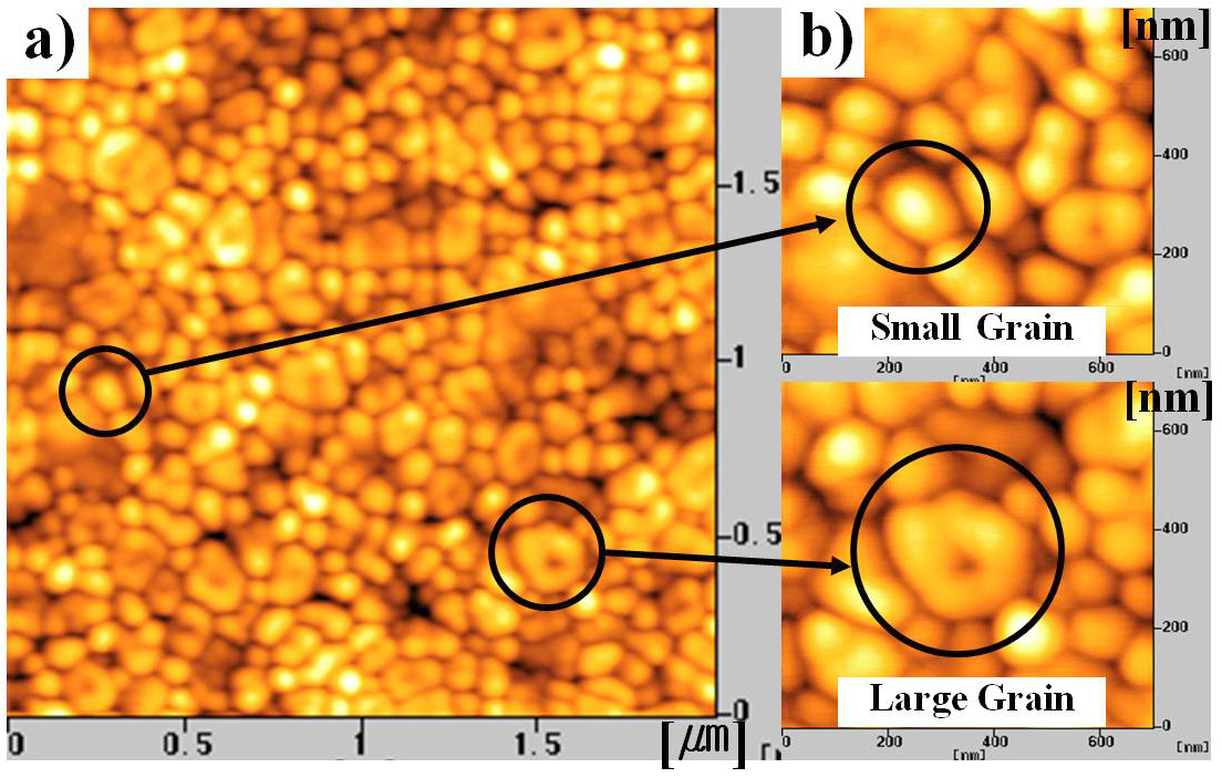
[Fig. 1.] (a) Topological image of selected small and large grains (b) magnified topological images.
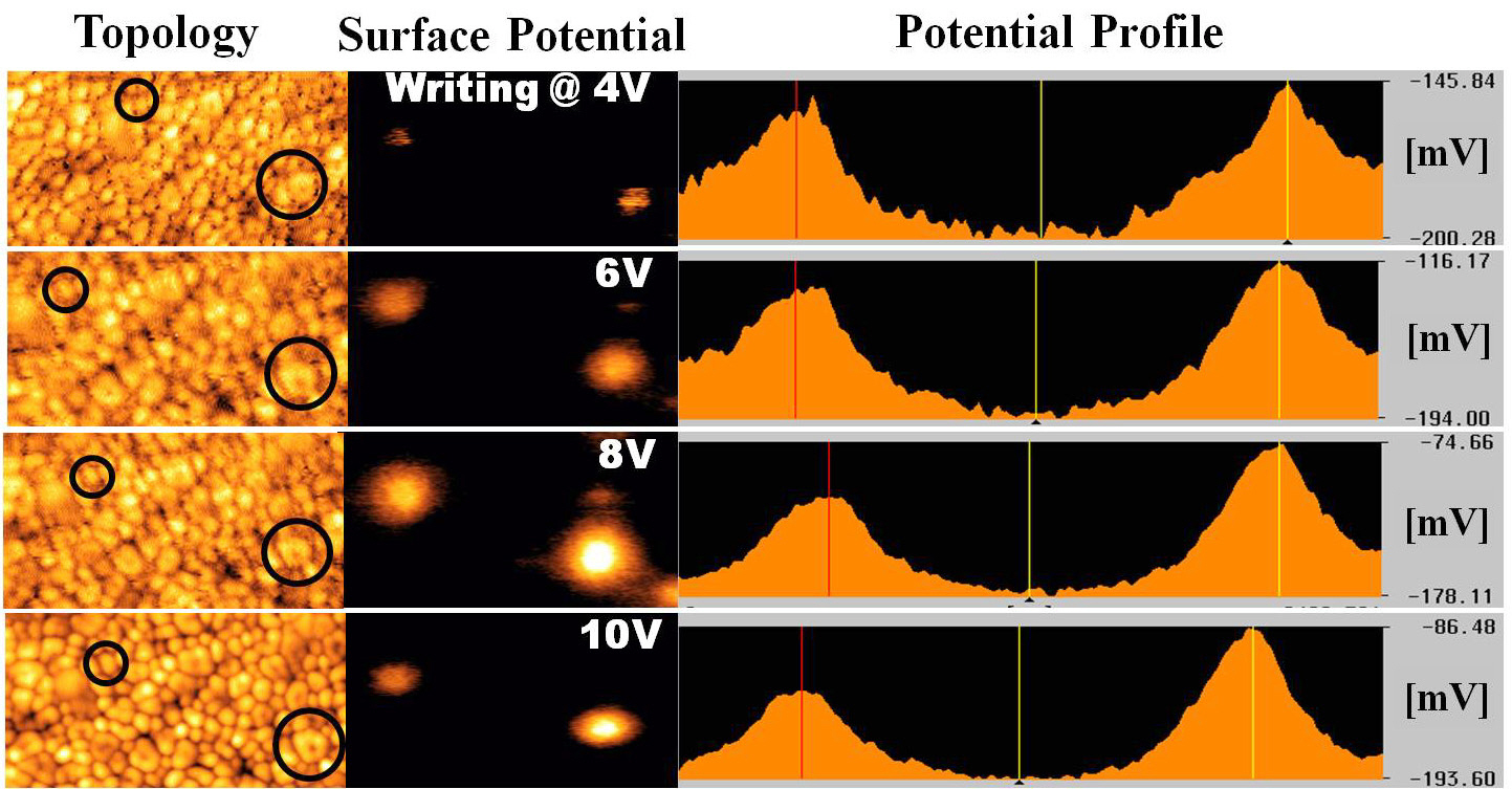
[Fig. 2.] Analysis of the topology and surface potential of PZT grains with Kelvin force microscopy.
the sol-gel method on to either a Pt/TiO2/SiO2/Si or IrO2/TiO2/SiO2/Si substrate. The PZT solutions were prepared from lead acetate trihydrate, titaniun tetra-iso-propoxide, zirconium tetran-propoxide, acetic acid and n-propanol. The composition of the solution was 0.4 mole Pb1.15Zr0.40Ti0.60O3.15, which is abbreviated as PZT (115/40/60). PZT sol-gel coatings were applied onto the substrate with an automatic spin coater. Then, the films were baked at 250-300℃ for 5 minutes in air on a hot plate and annealed in a 3-zone furnace at 650℃ in N2 atmosphere in order to prevent an additional chemical reaction at a high temperature. The procedure for measurement of the surface potential consisted of three sequential steps. First, the scan a certain area, namely, 5 ㎛ ×5 ㎛ to obtain a topological image of PZT film. After identifying the proper grains to investigate, write with a bias voltage to the selected small grain and large grain. Then, read the surface potential with an AC signal at a resonant frequency. The polarization writing procedure was performed in the contact atomic force microscopy (AFM) mode, whereas the reading was performed in the non-contact Kelvin force microscopy (KFM) mode. The DC voltage bias to the grains was applied by contacting a conductive cantilever to the center of the grain without scanning. The magnitudes of the bias voltages were varied from a -9 V to 9 V. The obtained surface potentials were used to plot the hysteretic behavior by relating it to the writing voltage. In addition, time dependent behavior of the surface potential was obtained by measuring the surface potential in terms of the elapsed time.In this study, we used a Seiko Instrument (model SPA 300; Tokyo, Japan).
Since the surface potential monitoring, utilizing KFM, pro-
vides information about the grain polarization, we carried out the detailed analysis for the grain polarization in terms of hysteretic behavior as well as time dependent behavior.
At first, we selected a proper grain in the topological image shown in Fig. 1(a). The circles represent the small grain and the large grain, respectively. The size of the small grain was 110 nm × 160 nm, whereas that of the large grain was 240 nm × 250 nm. The enlarged topological images are given in Fig. 1(b). The selected grains are biased using a 100 ms pulse with a voltage varying from 4 V to 10 V. The topological images and their surface potential images are given in the Fig. 2 with the analyzed profiles. As the poling voltage increases, the larger surface potentials appear in both the small and large grains. In addition, the difference of the surface potential between the large grain and the small grain is also increased as the poling voltage increases.
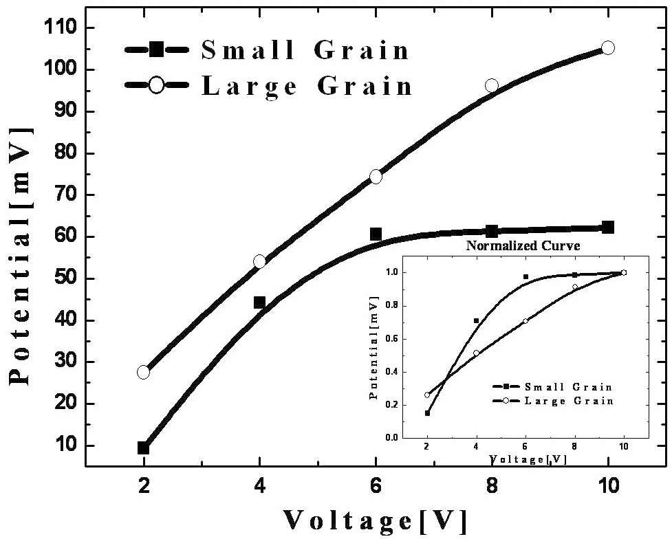
The surface potential response with respect to the poling voltage is given in Fig. 3. As shown in Fig. 3, the larger grain yields larger values of the surface potentials, whereas the smaller grain yields smaller values of the surface potentials. However, the smaller grain reveals a faster saturation trend than does the larger grain (see inset graph in Fig. 3). The inner plot represents the behavior normalized to the relative to the largest surface potential.
As expected, the faster response with respect to the poling
voltage appears in the small grain. It is not certain yet why the small grain shows an earlier saturation trend. However, one possible answer would be that the small grain tends to be a single domain and it causes a easily polling status, whereas the large grain does not.
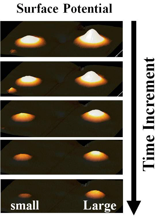
The time dependent behavior of the grain polarization was obtained by monitoring the surface potentials in terms of elapsed time. Figure 4 shows surface potential images obtained after the passage of time time. The images were obtained by measurement of the surface potential immediately after writing using 10 V with a 100 ms pulse width.
The bright region represents the negatively poled area where the dipoles are oriented upward. In other words, positively bound charge of the dipoles in the region should be on the surface.
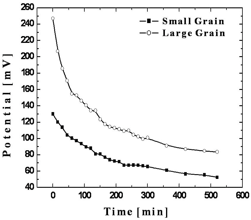
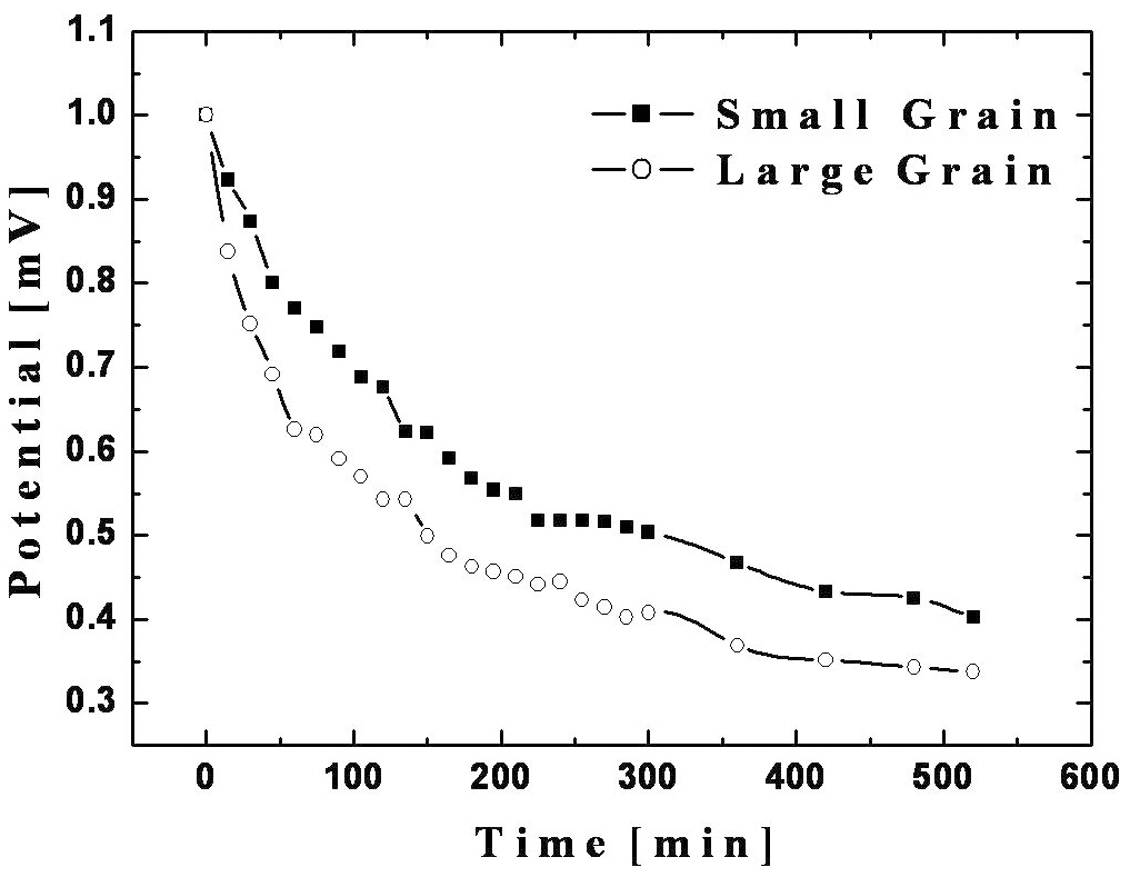
As shown in Fig. 4, the surface potential images become dark with increasing time for both the small grain and the large grain. When the peak surface potentials of Fig. 4 are plotted as the function of elapsed time, the surface potential reveals an exponential decay as given in Fig. 5. Both the small grain and the large grain show a similar decay trend. However, the normalized decay rate indicates that the smaller grain yields produce a slower decay as shown in Fig. 6. This result implies that although
the polling time for the small grain is faster than that of the large grain, the amount of polled domain are also smaller than that of large one.
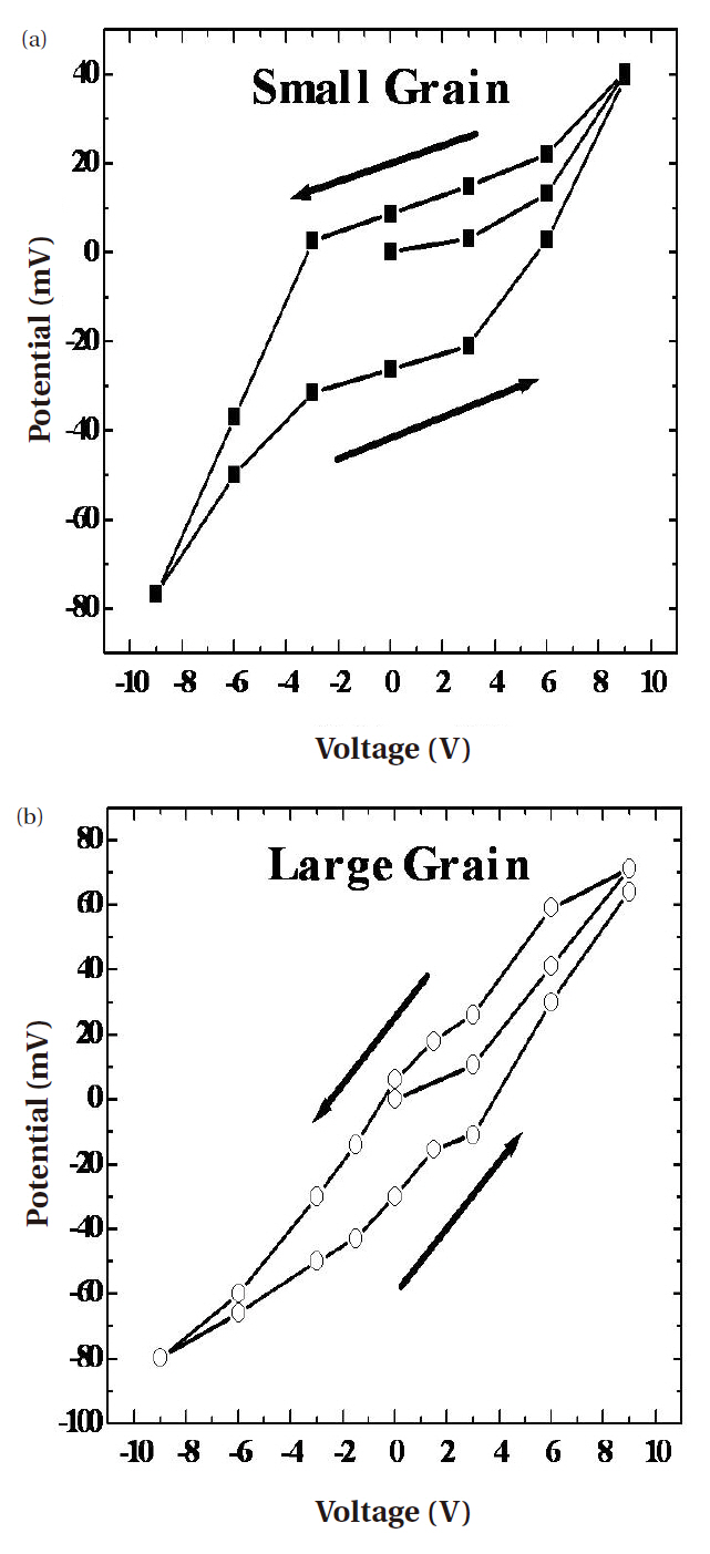
The previous studies indicate that the hysteretic behavior was obtained when the surface potential was plotted in terms of the writing voltage [1]. Since the hysteretic behavior of the PZT grain provides useful information related with the ferroelectric polarization, we attempted to plot the hysteretic behaviour of the PZT grains. The writing voltage was changed from -9 V to 9 V with 3 V intervals. As shown in Fig. 7, hysteretic behaviors were obtained from both the small grain and the large grain. The hysteretic behavior that we observed from the small grain is quite different from that observed from the large grain. If we try to understand this result on the basis of a conventional hysteresis loop, the large grain yields a larger remanant surface potential as well as a larger coercive voltage. Here it reminds us is that Ti rich PZT film usually gives larger coercive voltage and a larger remanant polarization value. At present, we are not sure about the existence of stoichiometry variation between the small grain and the large grain. However, the hysteretic behavior and time dependent behavior of the small grain looks better than those of the large grain. Thus, a possible variation in the stoichiometry can be a possible explanation. Another possible reason is the difference in the domain structure, namely, the existence of both a single domain and a multi-domain. It is necessary to investigate these considerations further.
We have examined the ferroelectric properties of PZT grains by monitoring of the surface potential. Hysteretic and time dependent behaviors of small grains were compared with those of the larger grain. The smaller grain yields smaller values of the surface potential. However, the normalize voltage versus surface potential behavior indicates an earlier saturation with respect to writing voltages. On the other hand, the surface potential hysteresis loop obtained from the smaller grain shows a similar shape that might be obtained from Zr rich PZT film, whereas the hysteresis loop of the larger grain looks like that obtained from a Ti-rich film. In addition, the time dependent behavior of the smaller grains also reveals a better response than those of the larger grains. The overll ferroelectric property of smaller grain seems to be better than that of the larger grain. At present, it is not certain whether the differences are due to t variation in the stoichiometry between Zr and Ti or the difference in the domain structure. It is necessary to investigate these facts further.