We examined the tunneling current behaviors of magnetic tunneling junction (MTJ) cells utilizing conductive atomic force microscopy (AFM) interfaced with an external magnetic field generator. By introducing current through coils, a magnetic field was generated and then controlled by a current feedback circuit. This enabled the characterization of the tunneling current under various magnetic fields. The current-voltage (I-V) property was measured using a contact mode AFM with a metal coated conducting cantilever at a specific magnetic field intensity. The obtained magnetoresistance (MR) ratios of the MTJ cells were about 21% with no variation seen from the different sized MTJ cells; the value of resistance × area (RA) were 8.5 K-12.5 K (Ω㎛2). Since scanning probe microscopy (SPM) performs an I-V behavior analysis of ultra small size without an extra electrode, we believe that this novel characterization method utilizing an SPM will give a great benefit in characterizing MTJ cells. This novel method gives us the possibility to measure the electrical properties of ultra small MTJ cells, namely below 0.1 ㎛ × 0.1 ㎛.
Since magnetic random access memory has promising aspects for next generation non-volatile memory, it has recently received growing interest [1,2]. In spite of its various advantages, some issues still remain to be solved for the integration of a magnetic spin junction with the standard silicon processes. In particular, as the size of an magnetic tunneling junction (MTJ) cell decreases, its switching field and magnetization vortex tends to increase [3,4], thereby becoming a serious bottleneck in realizing a gigabit scale. Besides the aforementioned issue, the anomalous switching behavior problem dependant on the shape of the inplane MTJ must be solved [5]. A novel characterization method is also demanded in order to evaluate a sub-micron size MTJ cell in terms of its current-voltage (I-V) behavior and magnetic domain image. With this in mind, we examined a novel technique used to evaluate the tunneling current behaviors of sub-micron size MTJ cells. We believe that this is a very important tool needed to monitor and evaluate the MTJ process, because it can determine the I-V curves of a MTJ cell under various magnetic fields without forming metal pads in a later process.
We interfaced an external magnetic field generating system with an scanning probe microscopy (SPM) in order to apply longitudinal magnetic fields to the cells. The magnetic field was generated by current flowing through coils and controlled by a current feedback circuit. The magnetic field direction (N or S) was determined by the current flow direction. The I-V measurement was carried out with a conductive atomic force microscopy (AFM) by applying a DC voltage between the Au coated cantilever tip and the bottom electrode of a MTJ cell. The MTJ cells that were used in this study consist of a pinned layer, a plasma oxidized Al2O3 layer, and a free layer. The Al2O3 was prepared on a sputter deposited CoFe/Ru/CoFe SAF layer. Then, a CoFe/NiFe ferro-magnetic layer was deposited onto the Al2O3/CoFe /Ru/CoFe layer. The role of the SAF layer in a MTJ structure is to
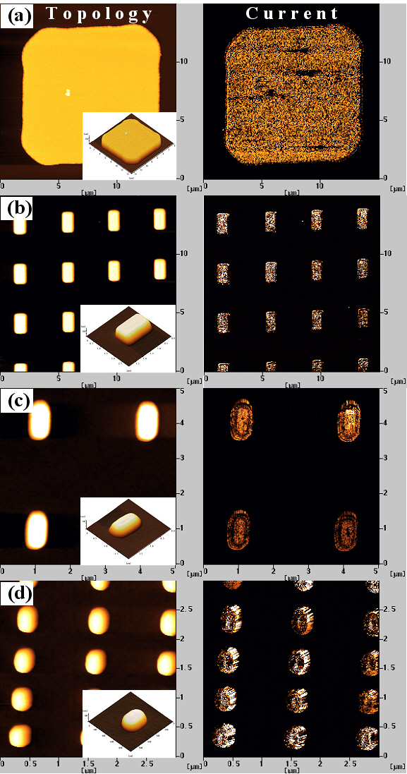
strictly fix the magnetization direction of the pinned layer by using an exchanging bias effect [6,7]. The different sizes of MTJ cells are 30 ㎛ × 30 ㎛, 10 ㎛ × 10 ㎛, 1.6 ㎛ × 0.8 ㎛, 0.8 ㎛× 0.4 ㎛ and 0.4 ㎛ × 0.2 ㎛. The Au-coated Si cantilever with a spring constant of 3 N/m was used to measure the tunneling current. At first, a wide area scanning was carried out with a 0.5 Vdc bias in order to verify the conducting status of the MTJ cells. The topology and current images were obtained simultaneously,as shown in Fig. 1. In the current image, a bright area represents a high conductance whereas a dark area indicates a low conductance.
One of the cells that conducted well was selected form the obtained current images, and magnified by rescanning using a smaller scan area. After confirming the current image of the MTJ cell, we placed the tip on the top electrode of the selected MTJ cell, and measured the spin polarized current behavior through the selected MTJ cell by sweeping the dc voltage, creating variable magnetic fields. Since the cells were exposed to a lateral magnetic field during the measurement, the magnetization direction in the free layer can be switched from a parallel state to an anti-parallel state or vice versa by changing the direction of the current flow through the coil. In this study, we used Seiko Instrument, model SPM 300 (Tokyo, Japan), interfaced with the external magnetic field generator in order to obtain current images as along with the magnetic force microscopy (MFM) images.
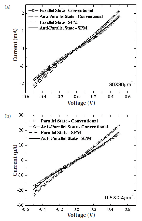
The MTJ cells were identified from the images obtained by the AFM. The topology and the current images were simultaneously obtained by scanning at 0.5 Vdc, as shown in Fig. 1. One of the best conducting cells was selected, and rescanned under a smaller scan area for a detailed analysis. The bright spots in the current image indicate the flow of more vertical current through the MTJ cell when compared to the dark area. After confirming the current image of the MTJ cell, we measured the tunneling current of the cell by applying a sweeping DC voltage under a variable magnetic field. The I-V curves obtained using the SPM are compared in Fig. 2 with those obtained using the conventional measurement system using a tungsten tip. The I-V curves obtained from the 30 ㎛ × 30 ㎛ MTJ cell show large differences in current.
The differences tend to increase as the applied voltage increases.This difference is attributed to the voltage drop in the SPM node, since the resistance of the SPM is about 100 Ω. If the resistance of the MTJ cell is comparable to that of the SPM, the voltage drop in the SPM node can not be neglected; it gives a lower current value. However, the voltage drop due to SPM resistance will effectively disappear when the area of the MTJ cell is reduced to submicron size because the resistance of the MTJ cell is inversely proportional to the area of the MTJ cell. In Fig. 2(b), the I-V behaviors of the 0.8 ㎛ × 0.4 ㎛ MTJ cell are compared to those obtained using the conventional method. As shown in the figure, no noticable difference was observed. The difference between the MR ratios obtained by each method seems to be negligible within the limits of experimental error, thereby indi-
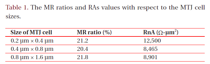
[Table 1.] The MR ratios and RAs values with respect to the MTJ cell sizes.

The MR ratios and RAs values with respect to the MTJ cell sizes.
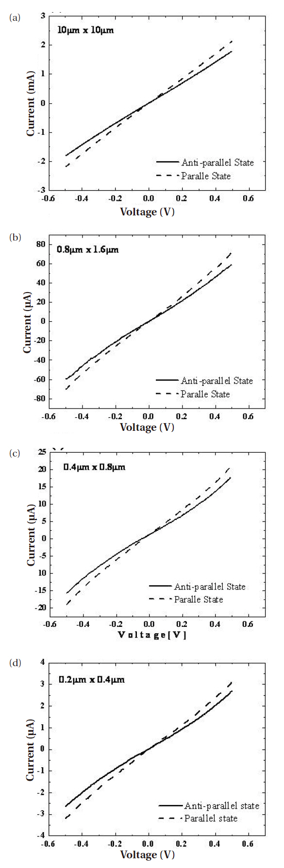
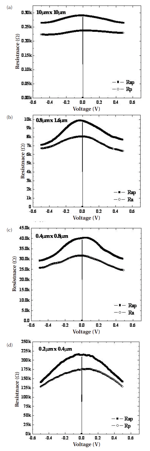
cating that the aforementioned explanation works quite well. Figure 3 shows the various I-V curves obtained from the different sized MTJ cells with different magnetized states in the free layer. As expected, the retarded conductions in the vertical current flow appeared in the anti-parallel cases. This trend is common to all of the samples we studied. Furthermore, the I-V behaviors shown in Fig. 3 reveal quite similar shapes, even though the size of the MTJ cell changed. The magnetoresistance (MR) ratio of the MTJ cell corresponds to the slopes of the I-V curves at a given voltage under a constant magnetic field. The influence of the contact resistance between the SPM tip and the top surface of the MTJ junction is negligible when the MTJ cell is small, and therefore the slope of the I-V curve represents the actual tunneling resistance in either the parallel state or anti-parallel state. We calculated the resistances of the MTJ cells at different voltages, and plotted those with respect to the bias voltages.
As shown in Fig. 4, the resistances of the MTJ cells yield a maximum value near 0V, and tend to decrease as the bias voltage increases in the parallel cases as well as in the anti-parallel cases.This tendency occurs similarly in all of the samples. For example,in the 0.2 ㎛ × 0.4 ㎛ MTJ cell, the calculated MR ratio at 0.5 V was around 21.2%. The variation of the MR ratios with respect to the size of the MTJ cell is given in Table 1. The MR values obtained at the bias voltage of 0.5 V are not changed even though the cell size is reduced. The obtained value of resistance × area (RA), which represent the resistance value multiplied by the area,were in the range of 8.5 K-12.5 K (Ω㎛2). As the cell dimension is reduced, the tunneling currents are also reduced, due to the smaller conducting area, thereby increasing the resistance. However, the increase in the resistance would be compensated for by the decrease in the area. The slightly larger value of RA in the 0.2 ㎛ × 0.4 ㎛ MTJ cell can be attributed to an additional resistance contribution from process factors, such as etching damage. However, this observation is quite consistent with the results reported in Parkin et al. [1]. Therefore, we believe that the characterization method utilizing the SPM seems to be quite useful in analyzing the electrical and magnetic properties of a MTJ cell under a controllable magnetic field. As a bonus, we can evaluate the etching damage incurred in the MTJ process by measuring its characteristics using this method.
In this study, we examined a novel method used to measure tunneling currents of sub-micron size MTJ cells. The conducting cantilever was brought in contact with the surface of the top electrode of the MTJ cells. The tunneling currents through the MTJ cells were measured by sweeping dc voltage from -1 V to 1 V under parallel and anti-parallel conditions. The obtained MR ratios yield almost a constant value, namely 21% regardless the MTJ cell size. Though factors, such as contact resistance, oxidation by tip bias, and equipment impedance, lead to deviations in the electrical characteristics of the MTJs, it seems to be negligible,especially at the smaller cell sizes. Thus, we believe that this novel method is a very effective tool to monitor and evaluate the MTJ process, because it can obtain the I-V curves of an MTJ cell under a magnetic field without forming a metallic pad to probe it. Further studies, including dynamic domain motion and the measurement of the H-R curve, are planned in order to obtain a detailed quantitative analysis of an MTJ cell.