Amorphous silicon thin film transistors (a-Si TFTs) are widely used for consumer electronics and have been demonstrated to be useful for use in solar cells and flexible displays. Organic thin film transistors are of interest for applications in low-cost electronic devices such as radio-frequency identification tags, flexible displays, memory and sensors. However, the applications of these devices are limited by their low mobility and light/moisture sensitivity due to intrinsic material properties Recently, zinc oxide (ZnO) has drawn much attention as one of the promising II-VI compound semiconductors that exhibits a wide band gap of 3.35 eV and a wurtzite structure; it can be used to form transparent electrodes, gas sensors, photovoltaic devices, light emitters, and bulk acoustic wave devices [1]. ZnO TFTs prepared by different techniques have been reported previously, mostly using inorganic dielectrics such as aluminum oxide [2-6]. The use of organic dielectrics for TFTs is likely to be an ideal solution for all-organic electronics. However, there have been few reports on oxide semiconductors used with a polymeric gate dielectric produced by atomic layer deposition (ALD) technology before the recent report [7]. In the case of organic gate dielectrics, the threshold voltage shift and hysteresis behaviors are unstable due to their structural imperfections and moisture absorption. In order to find a suitable dielectric system, polymer and high-k oxide double layer dielectrics could be used for TFT applications.
In this work, a bottom-gate and bottom-contact ZnO TFT prepared from ALD with a polymeric dielectric and silicon oxide hybrid materials was fabricated in order to investigate the effect of the hydrophobocity of the gate insulator on the TFT properties.The hysteresis behavior of this TFT was examined.
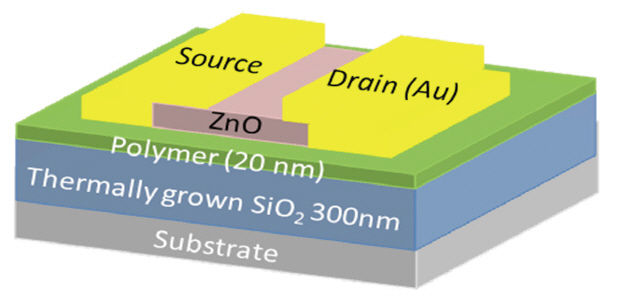
The bottom-gate and bottom-contact ZnO TFT used for this work a is shown in a schematic view in Fig 1. Poly(4-dimethylsilyl styrene) (Si-PS) was spin coated with a photo-crosslinking agent, in propylene glycolmonomethyl ether acetate on an silicon wafer that had been thermally grown and consisted of a silicon oxide film of 300 nm. The film was exposed to ultraviolet light (254 nm and 50 W of power) (using a G15T8, Sanyo Denki source, Tokyo,
Japan) to induce photocrosslinking. The thickness of the resultant film was found to be between 20-30 nm (using an Alphastep 500; KLA Tencor instrument, Milpitas, CA, USA) In the case of the polyimide, the polyimide solution was spin coated on to the thermally grown SiO2. The polyimide could be obtained by thermal curing of the coated film with a temperature of 150℃ for 30 minutes, 200℃ for 30 minutes and 250℃ for 60 minutes. The ZnO thin film used as a channel material was deposited on the cleaned substrate by the use of ALD with an injection type source delivery system at a temperature of 150℃. As a source of Zn, diethylzinc was used with gas purging at 100 sccm. During the reaction, diethylzinc and the oxygen plasma were sequentially injected into the reactor chamber to form a ZnO monolayer on the substrate. The thickness of the active layer was 20 nm, and the active layer was patterned by the use of photolithography. Gold as a source and a drain was deposited on the substrate by use of a thermal evaporator with a metal mask. The thicknesses of the source and the drain were 100 nm. All current voltage (I-V) characterizations of the ZnO TFT were carried out with a semiconductor parameter analyzer (Keithley 2400 and 236 Source meter, Cleveland, OH, USA) in the dark at room temperature.
In order to make oxide TFTs with bottom-contact and bottomgates,as shown in Fig. 1, indium tin oxide (ITO) and gold (Au) were used as electrode materials for gate and source/drain, respectively. A ZnO channel layer for bottom-contact thin-film transistors (TFTs) was prepared by the use of an injector type source delivery system ALD system. The average growth rate was relatively normal, about 2.0 A°/cycle.
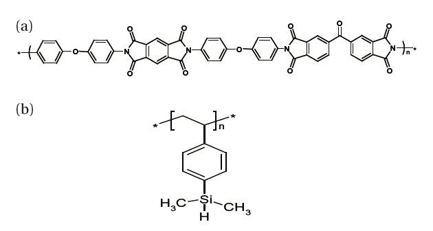
The dielectric materials for the hybrid structure consisted of two kinds, one type was composed of photocrosslinked poly(4-dimethylsilyl styrene) and (Si-PS) /silicon oxide. The other kind was a polyimide/silicon oxide as shown in Fig. 2. These materials were spin coated on to the thermally-grown silicon oxide silicon wafer, and then crosslinked for curing. The contact angle test was performed to investigate the surface polarity. The Si-PS composition showed a 99° angle with a high hydrophobicity, and the polyimide material showed a 68° angle with relatively hydrophilic characteristics. The difference in the hydrophobicity is due to the hydrophobic character of Si-moiety in Si-PS and the hydrophilic character of imide-moiety in polyimide. The properties of the ZnO TFT may be influenced by the hydrophobicity and hydrophilicity of the gate oxide because of its intimate contact with the semiconductor layer to form a channel layer. Conventional high k inorganic gate dielectrics are used for ZnO TFTs with a thick film thickness used to avoid gate leakage. Organic gate dielectrics for ZnO TFTs showed an unstable threshold voltage shift and hysteresis behavior due to their structural imperfections and moisture absorption. Because the surface roughness and
morphology of the dielectric surface is important, the surface can be modified by use of a self assembled monolayer. A dielectric surface has also been modified by deposition of a secondary polymer film onto a primary inorganic gate dielectric in order to make a hybrid dielectric layer.
In general, the capacitance of thermally grown silicon oxide is about 8-10 nFcm-2. The hybrid gate dielectric system of Si-PS/SiO2 and polyimide/SiO2 showed capacitances of 9.2 and 9.5 nFcm-2, respectively. The capacitance of the hybrid structure (polymer/ silicon oxide) of the dielectric is almost identical to that of a 300 nm thick bare SiO2 dielectric. This result arises because the very thin polymeric layer does not affect the overall capacitance of the gate dielectric. A similar result was reported for a polymer/silicon oxide bilayer used in a pentacene TFT [8]. Polystyrene, poly(4-hydroxyl styrene), and poly(4-vinyl pyridine) thin films on silicon oxide showed that the overall capacitance for all three bilayer gate dielectrics is almost identical to that of a base SiO2 insulator. In the case of the pentacene-based TFT prepared with hybrid gate dielectrics composed of poly(4-vinyl phenol) and a high k yttrium oxide system, high capacitance values and improved dielectric strength was exhibited in comparison with a poly(4-vinylphenol) only dielectric [9].
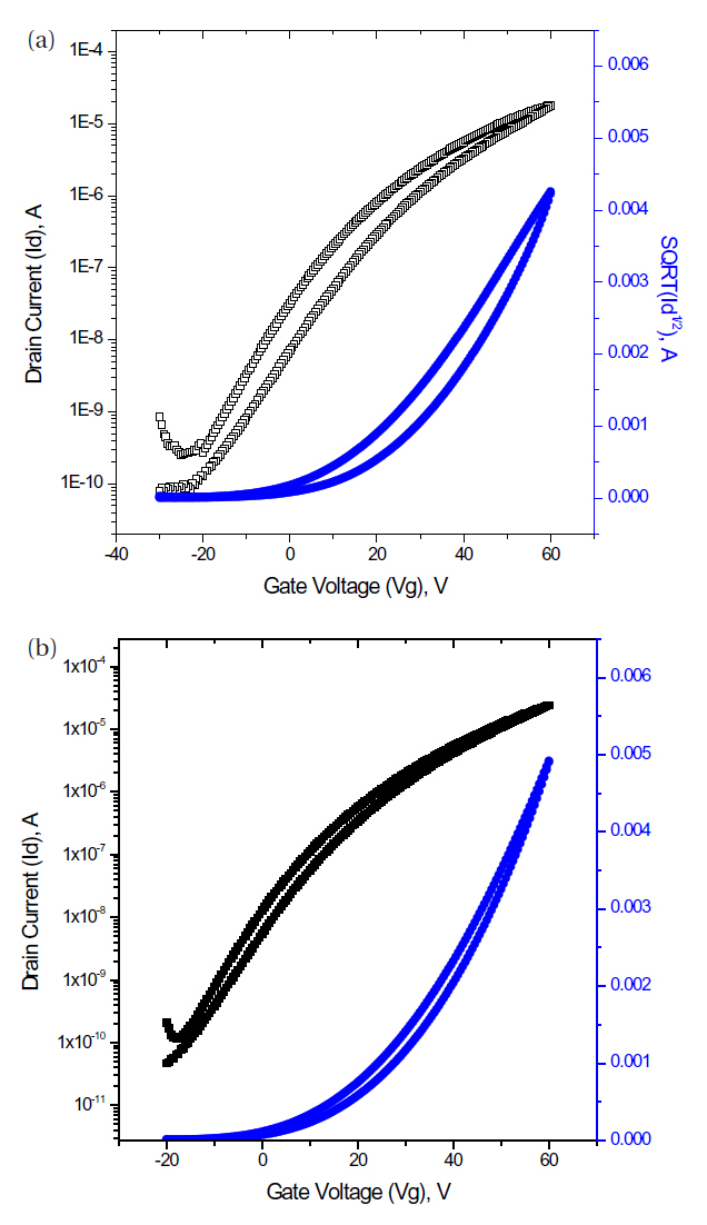
TFT parameters were obtained from Fig. 3. The threshold voltage was determined from an (Id)1/2 vs. Vg plot and the mobility was determined from a saturation calculation. The mobilities and threshold voltages of ZnO TFTs with a polyimide / SiO2 gate dielectric and poly(4-dimethylsilyl styrene) / silicon hybrid gate dielectric showed values of 0.2 cm2/Vs and 15.7 V, and 0.41 cm2/Vs and 24.4 V, respectively. This mobility is similar to that was obtained in our previous result for of the ALD-grown ZnO TFT with poly(4-vinylphenol) [7]. However, the threshold voltages of 15.7 and 24 V are shifted strongly towards the positive region.
In the case of a hysteresis test by forward and backward scanning of the gate voltage, the hysteresis of bottom contact TFT with a hybrid dielectric showed a highly improved characteristic comparing to that of the silicon oxide dielectric or polymeric dielectric. In general, the ALD-prepared ZnO TFT showed a negative bias shift. This shift in a minus direction is due to the free carrier density in ZnO derived from various sources, such as oxygen vacancies, zinc interstitials and hydrogen incorporations,and an intrinsic property of the gate dielectric, the interface effect between the oxide semiconductor and the polymeric dielectric[10]. The PVP gate dielectric showed an electrical instability due to the migration of ions and moisture-induced surface polarization under a negative bias [11]. In order to overcome this difficulty, most oxide semiconductor were subject to thermal treatment for several hours. However, we can obtain a much improved result with very low hysteresis transfer characteristics with a hybrid dielectric system of poly(4-dimethylsilyl styrene). The on-off ratio is over 106. This ratio is much higher than the ratio obtained with a ZnO TFT with a silicon oxide dielectric alone.
The functionality of chemical end groups in gate dielectric layers of polymers plays an important role in the determination surface hydrophobicity, that can also influence the semiconductor/dielectric interface properties, such as morphology and charge traps.
The Si-PS/SiO2 system exhibits a more hydrophobic characteristic compared to the polyimide/SiO2 composition, which implies that moisture absorption on the dielectric surface and moisture diffusion into the bulk sample are less likely to happen with a hydrophobic surface. The better hysteresis behavior associated with the more hydrophobic Si-PS system is due less absorption of moisture and less diffusion into the bulk of the sample. The water molecules at the interface between the semiconductor and dielectric can create long-lived acceptor or donor like traps in the band gap, which results in the hysteresis behavior of the drain current (Id) in the transfer characteristic.
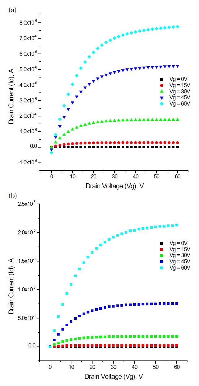
The output characteristic of the ZnO TFTs displayed solid saturation behaviors, as shown in Fig. 4. From the output characteristic,we find no current crowding, indicating a good contact resistance for the source-to-drain conduction. The output curves measured in the range Vd from 0 to 60 V, exhibit clear pinch-off and solid saturation. Therefore, the ZnO-TFT with a hybrid dielectric layer indicate that the device follows the standard fieldeffect transistor behaviour and that the Fermi level in the chan-
nel is controlled by the gate voltage and the drain bias.
ALD-grown ZnO bottom-contact TFTs have been prepared by the use of an injector type source delivery system. A hybrid gate oxide of photocrosslinked poly(4-dimethylsilyl styrene) (Si-PS) and silicon oxide for the TFT demonstrated a much improved hysteresis behavior. The mobility and threshold voltage of the ZnO TFT with poly(4-dimethylsilyl styrene) /silicon oxide hybrid gate dielectric showed values of 0.41 cm2/Vs and 24.4 V, respectively. The output characteristic is demonstrated with solid saturation behaviors.