Complementary metal-oxide-semiconductor (CMOS) technology scaling has been a main key for continuous progress in silicon-based semiconductor industry over the past three decades. However, as the technology scaling enters nanometer regime, CMOS devices are facing many serious problems such as increased leakage currents, difficulty on increase of on-current, large parameter variations, low reliability and yield, increase in manufacturing cost, and etc. To sustain the historical improvements, various innovations in CMOS materials and device structures have been researched and introduced. In parallel with those researches, various new nanoelectronic devices, so called "Beyond CMOS Devices," are actively being investigated and researched to supplement or possibly replace ultimately scaled conventional CMOS devices. While those nanoelectronic devices offer ultra-high density system integration, they are still in a premature stage having many critical issues such as high variations and deteriorated reliability. The practical realization of those promising technologies requires extensive researches from device to system architecture level. In this paper, the current researches and challenges on nanoelectronics are reviewed and critical tasks are summarized from device level to circuit design/CAD domain to better prepare for the forthcoming technologies.
The relentless evolution of electronics, information technology (IT), and communications has been mainly enabled by continuous progress in silicon-based complementary metal-oxidesemiconductor (CMOS) technology. This continuous progress has been maintained mostly by its dimensional scaling, which results in exponential growth in both device density and performance. The reduction in cost-per-function has steadily been increasing the economic productivity with every new technology generation. In addition to its scalability, the unique device properties such as high input resistance, self isolation, zero static power dissipation, simple layout and process steps have made CMOS transistors as the main components of the current integrated circuits (ICs). Today CMOS ICs are everywhere and indispensible in our life, ranging from portable electronics to telecommunications and transportation [1].
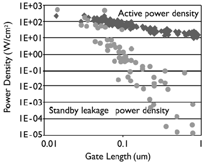
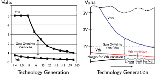
However, as device scaling continues for the 21st century, it turns out that the historical growth, doubled circuit density and increased performance by about 40% every technology generation, followed by "Moore's Law," [2, 3] cannot be maintained only by the conventional scaling theory. Increasing leakage current does not allow further reduction of threshold voltage, which in turn impedes further supply voltage scaling for the historical speed improvement. Accordingly, generated higher electric fields inside of the transistor worsen device reliability and increase leakage currents. Moreover, the required high channel doping causes significant challenges such as mobility degradation, increased band-to-band tunneling (BTBT), gate-induced drain leakage (GIDL) and random dopants induced threshold voltage fluctuations [4].
Due to those ever increasing short channel effects (SCEs), there have been several strategies introduced for CMOS device to extend Moore's Law. A few examples of those are; increasing electrostatic control over the channel by means of the continuous equivalent oxide thickness (EOT) scaling with high-k/metal gate stack, multi-gate structures for higher drive current at the constant over-drive voltage, improving carrier mobility by adopting high mobility channel materials, and strain engineering and reducing parasitics.
In addition, various researches have been actively carried out in device domain to find an alternative device to continue to sustain Moore's Law. Among these efforts, various kinds of alternative memory and logic devices (beyond CMOS devices) have been proposed. These nanodevices take advantages of the quantum mechanical phenomena and ballistic transport characteristics under low supply voltage and consume low power. Furthermore, due to their extremely small sizes, those devices are expected to be used for ultra-high density integrated electronic components having billions of devices in a single chip. However, it also increases defects and variations both during manufacture and chip operations.
In the introductory part of this paper, after the CMOS technology scaling trend and "Small-Geometry Effects" are reviewed to understand what impedes further down-scaling of planar bulk metal-oxide-semiconductor field-effect transistors (MOSFETs), the current and tentative efforts to cope with the limiting factors are discussed. After the CMOS scaling issues are reviewed, present and promising nanotechnology devices such as siliconon- insulator (SOI) devices, Multi-gate FETs, Si nanowire/cabon nanotube FETs are investigates in terms of their advantages/ drawbacks, basic operation principles, current state of development, and challenges for commercialization along with other possible options. Finally, this paper will conclude with a discussion of the various challenges to be resolved for nanoelectronics to be a full-brown technology from device to system architecture level.
2. CHALLENGES FOR NANOSCALE MOSFETs
It is important to have a solid understanding of the phenomena that occurs in nanoscale MOSFETs since it not only provides useful interpretation of the anomalies that we might encounter in their SPICE simulations but also provides us the future possibilities and limitations of the device scaling. In this section, we will review these phenomena starting from a brief overview of scaling trend of silicon-based planar bulk MOSFETs and highlight the challenges to be solved. Current approaches to control these small-geometry effects such as increased leakage currents, threshold voltage variations, weakened gate controllability over the channel, and increased in S/D resistances will be discussed.
Since the first MOSFET was successfully demonstrated in 1960 [5], in order to keep up with the increasing demand for faster, smaller, and cheaper products, lots of efforts have been made to shrink the size of MOSFET switching devices in semiconductor industry. Without any significant fundamental changes, the basic structure of MOSFETs has been evolved to continue its successful geometric scaling. The fundamental principles to scale down devices have been guided by the ideal scaling principles formulated by Robert Dennard in 1974 [6], and it is based on a simple electrostatics; if the device dimensions (
2.2 Issues for nanoscale MOSFETs: Categorized based on where the problems occur
2.2.1 Channel
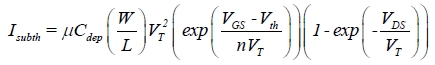
where (특수문자) denotes the capacitance of the depletion region under the gate area, VT is the thermal voltage which equals to kT/q, and n is the sub-threshold parameter and expressed as 1+Cdep/Cox. Since, from Eq. (1),
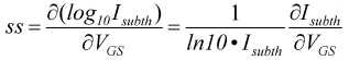
This parameter shows how abruptly the transistor turns off with decreasing gate voltage. In order to turn off the transistor effectively,
The transistors with a different channel length (
If the depletion region around the drain continues to extend to the source depletion region with the further increasing drain voltage and finally merges together before junction breakdown occurs, the drain current increases due to the existence of a parasitic current path located well below the gate. This phenomenon is known as
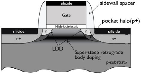
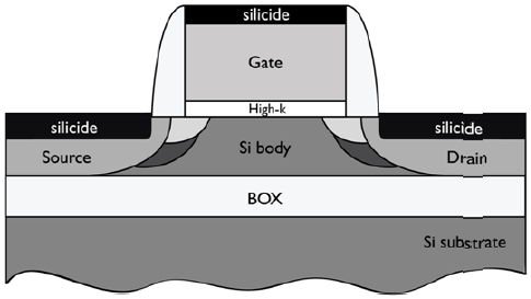
All these phenomena are collectively referred to as "shortchannel effects (SCEs)" and tend to increase standby leakage power dissipation. To mitigate SCEs, an advanced MOSFET, depicted in Fig. 5, uses the silicidation of S/D junctions and lightly doped drain/source (LDD) structure with pocket halo implant and super-steep retrograde body doping [12, 15-17].
Additionally, increasing random dopant variations (RDF) and line-edge roughness (LER), particularly non-rectangular gate can cause significant statistical
Another high electric field is developed between the gate and the channel due to the aggressive gate oxide thickness scaling with relatively constant supply voltage, which limits the charge carriers to a narrower region below the oxide-silicon interface, leading to more carrier scattering and hence lower mobility. Furthermore, the increased body doping by means of suppressing SCEs degrades the carrier mobility [21].
The lightly LDD MOSFETs, shown in Fig. 5, have been widely used to reduce the maximum longitudinal electric field in the channel by means of the additional voltage drop across the higher resistive LDD region. As a result, the LDD technique increases hot carrier immunity in a device, but also degrades the device performance [15, 21].
2.2.2 Gate
One of the key innovation enablers for 45 nm process technology and beyond is the high-k/metal gate transistor, which is regarded as one of the biggest developments in transistor design in 40 years [25]. High-k/metal gate have enabled the continuous EOT scaling. In this section, the motivation for using high-k/ metal gate stack in advanced CMOS devices is discussed.
However, even heavily doped poly-Si gate electrode has a certain resistance which contributes to a considerable RC time delay. Furthermore, when the doping concentration of the poly- Si is not sufficient, at high gate bias during inversion, a region in the poly-Si gate electrode adjacent to the poly-Si/SiO2 interface becomes depleted with carriers, which is called "Poly-depletion Effect." This results in increased EOT and hence significant decrease in the drive capability of transistor. To improve gate depletion, the number of active dopants in the gate electrode can be increased, but this solution is limited as current doping concentrations are already nearing the equilibrium solid solubility in silicon [27, 28].
For these reasons poly-Si is not suitable for the future gate electrode and new materials are required. Fortunately, metal gate electrode with a suitable work function (WF) shows many advantages such as lower gate sheet resistance and no boron penetration and poly depletion effect. However, the selection of metal gate substitutes for poly-Si, which are compatible with the new high-k gate dielectrics, is not as advanced [29].
2.2.3 Drain/source
2.2.4 Substrate (bulk)
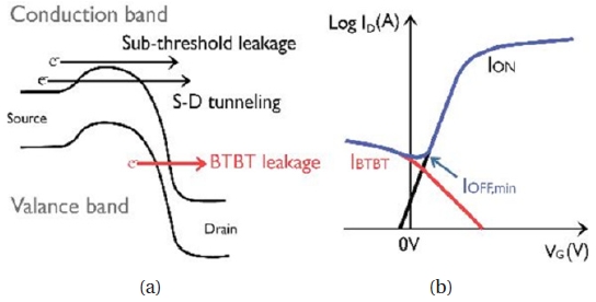
Substrate leakage current consists of impact ionization current, reverse-biased junction leakage current (mostly BTBT leakage current), and GIDL current.
Recently high-mobility channel materials, such as Ge, strained-Ge (s-Ge), s-SiGe, and III-V materials (GaAs, InAs, InSb, and InGaAs), are actively being researched as candidates for future channel materials of highly scaled MOSFETs. However, since most of high-mobility materials have lower band gaps than Si, BTBT leakage currents increase significantly. Therefore, various device structures to minimize BTBT currents are being developed [35]. The various leakage mechanisms in a MOSFET are illustrated in Fig. 6.
2.3 Summary
As the device scaling is approaching its physical size limitations, the technology cycle is getting slow down due to increasing power consumption, process variation, and fabrication cost. To continue the historical growth for the next decade, various studies have been conducted to overcome ever increasing challenges. As explained in section 2.1, nowadays device scaling tradeoffs between performance and power consumption, therefore technological innovations which can achieve high performance through very low power are required. These efforts have made conventional MOSFETs evolve in various ways with new materials, new structures, and so on. In the next section, the evolution of MOSFET structures is reviewed.
The conventional device scaling trend, which is mostly based on reducing its physical size, is no longer valid for the future technology generations. Therefore, several strategies have been introduced to extend Moore's Law, such as increasing electrostatic control over the channel by means of the continued EOT scaling with high-k/metal gate stack and multi gate structures for higher drive current at constant over- drive voltage (
The advantages of SOI technology come from its buried oxide (BOX) layer (a cross-section of a SOI device is shown in Fig. 7). With the reduction of the parasitic capacitances, mostly as a result of the reduced drain/source junction capacitances, SOI devices yield improved switching speed and reduced power consumption. The operating speed is also improved since the isolated channel from substrate bias prevents the increase in a threshold voltage of stacked SOI transistors. In addition, the perfect lateral and vertical isolation from substrate provides latchup and inter-device leakage free CMOS technology, reduction in various interferences, and better soft error immunity. Moreover, SOI technology offers tighter transistor packing density and simplified processing [39].
SOI transistors are classified into two types; "partially depleted (PD) SOI," if the silicon film (typically 100 nm or more) on the BOX layer is thicker than the depletion region depth beneath the gate oxide, and "fully depleted (FD) SOI," if the body (silicon film) thickness is thin enough (typically 50 nm or less) or the doping concentration of the body is low enough to be fully depleted. FD SOI transistors have superior advantages over PD SOI transistors in terms of extremely low sub-threshold swing (<65 mV/decade), no floating-body effects, and low threshold voltage variation with temperature (2-3 times less). However, since FD SOI transistors are even more sensitive to process variation such as the silicon film layer variation resulting in threshold voltage fluctuation, PD SOI devices were commercially introduced first. With careful device design and advanced process techniques, fully depleted ultrathin-body SOI (FD UTB SOI) devices are considered as one of the best scaling options. Undoped or very lightly doped UTB devices minimize impurity scattering and reduce threshold voltage variation resulting from random dopant fluctuation [40].
Another important merit of SOI technology is that it provides the cornerstone for new device structures such as multi gate field-effect transistors (MuGFETs), which includes more than one gate into a single device. The double-gate (DG) FET shown in Fig. 8(b) is the first step for those multi gate devices. Since the transverse electric field induced by
On the other hand there is a significant drawback in SOI technology. Since the BOX, which has approximately 100 times lower thermal conductivity than that of silicon, prevents thermal conduction path from SOI transistors to the substrate, SOI transistors are easily affected by the thermal heating generated in the channel, which is called "Self-Heating Effects." Consequently, the self-heating degrades the mobility of carriers and causes the threshold voltage shift. These effects get worse with FD structures because they use thinner silicon films [43].
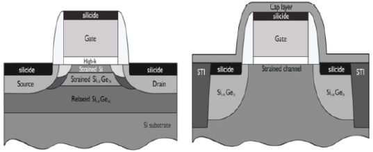
Mobility loss resulted from higher channel doping and scaled gate dielectrics should be compensated to meet the performance targets of the future technologies. In the parallel with SOI technology, there has been more straight forward and cost effective way to improve device performance and scalability. That is mobility-enhancement technology. Both the high mobility channel materials (such as Ge and GaAs) and the strained channel by means of stress offer mobility enhancement. Various CMOS fabrication processes can be used to induce appropriate strain to the channel region of the MOSFETs. Strain engineering can be largely divided into two: local strain and global strain. Local strain exploits the process steps such as shallow trench isolation (STI), silicidation at the source/drain (S/D) region, and nitride CESL (Contact Etch Stop Liners). The local strain techniques were first used because they were more promising for manufacturing. However, since they have strong device geometry dependence, it makes their scaling behavior less predictable. The most innovative way on strained-Si was focused on biaxial global strain generated by depositing a thin layer of silicon on a relaxed SiGe virtual substrate. This results in enhanced carrier transport in the strained Si layer, and mobility enhancements of 110% for electrons and 45% for holes. A cross-section of transistors with strained Si-channel fabricated by means of both the global and local strains is shown in Fig. 9 [44-46].
Appropriately applied strain to the MOSFET channel can significantly improve the device performance by means of modifying energy bands and increasing mobility of carriers in silicon. Strain is being widely used in HP logic technologies. SiGe in the PMOS S/D regions, stress memorization technique (SMT) for the NMOS, and a nitride stress-capping layer for both devices have been commonly employed in state-of-the-art MOSFETs since its introduction at the 90nm node. Strain is expected to continue CMOS technology scaling for the time being [47].
3.3 Possible solutions after CMOS scaling limits
As dimensional scaling of CMOS transistors is reaching their fundamental physical limits, various researches have been actively carried out to find an alternative way to continue to follow Moore's law. Among these efforts, various kinds of alternative memory and logic devices, so called "Beyond CMOS Devices," have been proposed. These nanodevices take advantage of the quantum mechanical phenomena and ballistic transport characteristics under lower supply voltage and hence low power consumption. Those devices are expected to be used for ultra high density integrated electronic computers due to their extremely small size. In the following sections, the general overview will be discussed for the promising emerging logic nanodevices such as nanowire (NW) transistors, carbon nanotube field-effect transistors (CNTFETs), graphene nanoribbon (GNR) transistors, single electron transistors (SETs), and quantum-dot cellular automata (QCA) in terms of their basic operation principles, current state of development, and challenges for commercialization.
4. PROMISING NANODEVICES BEYOND CMOS
There are a number of nanoelectronic devices that can possibly supplement or replace current CMOS devices. These include nanowire or carbon nanotube transistors, graphene FETs, single electron transistors, and spin transistors. These devices offer sizes of a few nanometers and can be self-assembled.
Nanowire field-effect transistors (NWFETs), gate-all-around or surround gate FETs with a thin nanowire channel, have drawn much attention and have been considered as promising candidates for continuous CMOS scaling since their nonplanar geometry provides superior electrostatic control of the channel than the conventional planar structures. The increasing attention in nanowire research stems from several key factors: their highyield reproducible electronic properties [48-50], cost-effective "bottom-up" fabrication which circumvents some fabrication challenges, higher carrier mobility by means of the reduction of scattering resulting from the crystalline structure, smooth surfaces and the ability to produce radial and axial nanowire heterostructures [51, 52], better scalability resulting from the fact that diameter of nanowires can be controlled down to well below 10 nm [53, 54].
However, due to their smaller nanowire diameters, the inversion charge changes from surface inversion to bulk inversion due to quantum confinement. Thus, variations in nanowire dimensions due to fabrication imperfections can lead to perturbations in the carrier potential and scattering that degrade the charge transport characteristics. Also, variations in nanowire diameters may lead to a variation in FET threshold voltage. Reducing variability is therefore a key challenge in making nanowire FETs a viable technology. Furthermore, quantum confinement effects make modeling of nanowire transistors a complex problem. While there are many studies in the literature on the modeling of nanowire transistors based on nonequilibrium Green function or Monte Carlo approaches, the physics related to the operation of nanowire transistors needs to be well articulated so that simple compact models, including ballistic transport and realistic subband parameters, can be developed for circuit design using SPICE-like simulators [55].
4.2 Carbon nanotube field-effect transistors (CNTFETs)
Since they were discovered in 1991 [56], due to their unique material properties [57], carbon nanotubes (CNTs) have received worldwide attention from many different fields of scientists and engineers.
CNTs are graphene, which is a two-dimensional honeycomb lattice of carbon atoms, sheets rolled up into cylinders. They show either metallic or semiconducting properties depending on the direction how CNT are rolled up (chirality). Since the bandgap of semiconducting CNTs is inversely proportional to their diameters, threshold voltage can be easily controlled [58-60].
With their superior material properties, such as large current carrying capacity, the excellent mechanical and thermal stability, and high thermal conductivity, the metallic nanotubes are attractive as future interconnects [61]. Along with these properties, the semiconducting nanotubes also show great advantages as a channel material of high-performance (HP) FETs. It is easier for CNTFETs to incorporate high-k dielectrics due to the absence of dangling bonds. Also, since both NMOS and PMOS transistors show almost identical I-V characteristics, it becomes a significant advantage for CMOS circuit design. Furthermore, they are very attractive to Si-based semiconductor industry for the following reasons: 1) CNTFETs show considerable improvement in device performance metrics such as low power and high speed 2) their operating principles and devices structure are similar to Si-based CMOS transistors; therefore, the CMOS design infrastructure could be reused [62].
Even though CNT-based electronics presents great promise, there are several difficult challenges to be solved. No existing processes for synthesis or growth of nanotubes can produce tubes with identical diameters and chiralities. The starting material will have to be purified if far more selective growth processes cannot be developed. Many progresses are being reported in purification. However, there is still a big gap between these promising early results and the extremely tight control of placement that would be needed. Furthermore, an even tighter gate control through ultrathin high-k gate dielectrics and extremely abrupt doping profiles are required for the device fabrication [63].
4.3 Graphene nanoribbon (GNR) transistor
Graphene, a single atomic layer of carbon atoms arranged into a two-dimensional (2D) hexagonal lattice, or simply thought as an unrolled CNT, shows great potential for nanoelectronic devices since its discovery in 2004 [64]. It shares many of the advantages of metallic CNTs such as the high carrier mobility for ballistic transport, high carrier velocity for fast switching, excellent thermal conductivity, and etc. The potential to produce wafer-scale graphene films with full planar processing for devices promises high integration potential with conventional CMOS fabrication processes, presenting a significant advantage over CNTs [65].
Two-dimensional graphene has a zero band-gap (EG) semimetal characteristic. However, by patterning graphene into a few nanometer wide GNR, a band-gap can be induced [66]. Similar to the CNT cases, GNRs have energy band-gap which is inversely proportional to their width, and width confinement down to the sub-10 nm scale is essential to open a band-gap that is sufficient for room temperature transistor operation. Unlike CNTs, which are mixtures of metallic and semiconducting materials, recent samples of chemically derived sub-10 nm GNRs have shown allsemiconducting behavior [67]. GNRs, under the assumption that the edges of ribbons are passivated by hydrogen atoms, have two main types of armchair-edge and zigzag-edge GNRs (AGNRs and ZGNRs). ZGNRs are predicted to be metallic by a simple tightbinding model, but a band-gap exists in more advanced and spin-unrestricted simulations [68]. For digital circuit applications, the focus has been on using AGNRs as the channel material. AGNRs have an electronic structure that is closely related to that of zigzag CNTs. The band-gap in AGNRs originates from quantum confinement, and edge effects play a critical role [68, 69].
Due to the atomically thin and nanometer-wide geometries of GNRs, variability and defects are projected to have a larger impact on GNRFET circuit performance and reliability in comparison to the conventional silicon devices. Variability, for example, can arise from the difficulty of control of the GNR width, edge roughness, or oxide thickness during fabrication. Defects may occur during fabrication due to a charge impurity in the gate insulator or a lattice vacancy, and result in a large performance variation or a nonfunctional device. Not only must each of the variability and defect mechanisms be identified and studied, the models developed for GNRs and GNRFETs must be capable of predicting their effects in isolation as well as together in a systematic manner [69].
Although the GNR material promises ultra-small, fast, and low-energy FETs, two key effects of variability and defects - leakage and low noise margins - are significant. For example, the variation of the channel width by a couple of angstrom changes the leakage current by orders of magnitude, and a single Coulomb charge impurity can lower the FET on-current by about 30%. Dense memories, which are the biggest prospect for graphene- based devices, are particularly susceptible to variations and defects with near-zero noise margins and an increase in leakage power of over 5 X. This assessment of the effects of variability, defects, and parasitics indicate their important role on circuit performance. These effects must be carefully considered in the performance assessment and design optimization for future graphene-based electronics technology [70].
4.4 Single-electron transistors (SETs)
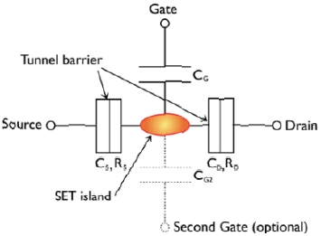
Due to their small size and low-power dissipation at good speed, SETs are very attractive devices for future large-scale integration. The basic structure of SET consists of three-terminals such as drain, gate, source, and the second gate is an optional. A schematic of SET, as shown in Fig. 10, is analogous to that of conventional MOSFETs. However, SET has a tiny conductive island coupled to a gate electrode with gate capacitance Cg. Source and drain electrodes are connected to the island through a tunnel barrier (junction). The tunnel barrier, which controls the motion of every single electron, consists of two conductors separated by thin layer and it is modeled as tunneling resistances RD, S and junction capacitances CD, S. The increased gate bias attracts electrons to the island only through either drain or source tunnel barrier, and the number of electrons in the island only has a fixed integer. Therefore, the increased gate bias makes electrons flow one by one when a small voltage is applied between the source and drain electrodes by means of the "Coulomb blockade" phenomenon [71-73].
New applications and architectures that exploit the unique functionality of room temperature operating SET circuits have been developed, especially by monolithic integration of SETs with FET circuits to complement the conventional Si CMOS performance. Representative examples include SET/CMOS hybrid multi-value logic circuits [74], multiband filtering circuits [75], analog pattern matching circuits (discussed more fully in the next section) [76], associative recognition tasks [77], and others [78], in which characteristic Coulomb blockade oscillations of SETs are typically utilized to reduce the number of devices. Note that certain aspects of the circuit performance, especially the room temperature operation [76, 79], already exceed the theoretical evaluation of the logic gate parameters for 2 nm SETs. These devices have a theoretically estimated maximum operation temperature T~20 K, integration density n~1011 cm-2, and speed of the order of 1 GHz [80]. However, large threshold voltage variation continues to impede the realization of large scale SET circuits, making it difficult for SETs to compete directly with CMOS devices used to implement Boolean logic operations. Engineering breakthroughs are needed to eliminate the size and background charge fluctuations in order to suppress the threshold voltage variations.
The majority of the SET circuits demonstrated to date employ so called "voltage state logic," where a bit is represented by the voltage of capacitor charged by many electrons. The problem of the low fan-out for this scheme can be overcome by reducing the capacitance and/or by combining with conventional FET circuits. Truly single-electron approaches, representing a bit by a single electron ("bit state logic") [81] and the use of a single electron as a source of random number generations [82], have been limited to laboratory demonstrations. The problem of the limited fan-out, which is caused by using only a single electron in the truly single-electron devices, may be solved by innovative circuit designs such as the binary-decision-diagram [83].
4.5 Quantum-dot cellular automata (QCA)
As the number of transistors placed onto a single chip increases, the heat generated during a switching cycle can no longer be removed and this may result in considerable limitation of the speed of operation. There is a new paradigm which takes advantage of the reduction of the feature size. One nanostructure paradigm, proposed by Lent et al. [84-86], is QCA, which exploits arrays of coupled quantum dots to implement Boolean logic functions. The advantage of QCA lies in the extremely high packing densities possible due to the small size of the dots, the simplified interconnection, and the extremely low power-delay product [87].
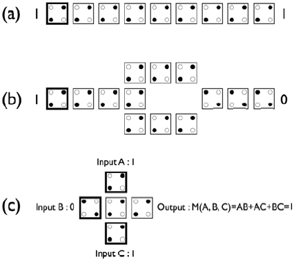
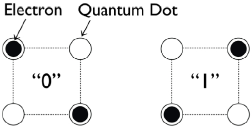
A schematic diagram of a four-dot QCA cell is shown in Fig. 11. This is the simplest non-clocked QCA cell. The cell consists of four quantum dots positioned at the comers of a square. The cell contains two extra mobile electrons, which are allowed to tunnel between neighboring sites of the cell, but not out of the cell. If the tunnel barriers between cells are sufficiently high, the electrons will be well localized on individual dots. The Coulomb repulsion between the electrons makes them occupy antipodal sites in the square as shown. For an isolated cell, there are two energetically equivalent arrangements, polarizations, of the extra electrons that we can denote as binary 1 and binary 0. The two polarization states of the cell will not be energetically equivalent if other cells are nearby, because the Coulomb interaction with other cells breaks the degeneracy [87].
A QCA wire is shown in Fig. 12(a). The left-most cell is fixed with polarization representing the input. The difference between input and outputs cells in QCA arrays is simply that inputs are fixed and outputs are free to change. The ground state configuration of the remaining free cells is the one with each cell polarized in the same way as the input cell. We can consider this transmission of the input signal from one end to the other. Cells that are positioned diagonally from each other tend to anti-align. This behavior is employed to construct an inverter as shown in Fig. 12(b). Fig. 12(c) shows the fundamental QCA logical device, a three-input majority gate, from which more complex circuits can be built. The central cell, labeled the device cell, has three fixed inputs labeled A, B, and C. The device cell has its lowest energy state if it assumes the polarization of the majority of the three input cells. It is possible to "reduce" a majority logic gate by fixing one of its three inputs in the 1 or 0 state. In this way, a reduced majority logic gate can also serve as a programmable AND/OR gate. Combined with the inverter shown above, this AND/OR functionality ensures that QCA devices provide logical completeness [87].
For practical QCA circuits, clocked control is necessary. In clocked circuits, the system is switched smoothly between the ground state corresponding to the old inputs and the state corresponding to the new inputs. Clocking allows cells to be locked in a particular state, performing as a latch. Thus general purpose computing is possible, and in particular, latches make it possible to implement pipelined architectures as required in all highperformance systems [88].
A severe problem of QCA arises from the fact that QCA are single-electron devices and they are very sensitive to the background charge. Today, no viable solutions to the background charge immune single-electron systems are known. Another serious drawback of QCA devices is that room-temperature operation is not achievable with solid-state QCA systems [79].
5. TECHNICAL CHALLENGES FOR ANOELECTRONICS
While nanoelectronics presents the opportunity to incorporate billions of devices into a single chip, it also increases defects and variations both during manufacture and chip operations. In this chapter, technical challenges are summarized for nanoelectronics technology ranging from device to system architecture level.
Due to their extremely small size (tens of nanometers and below), quantum-mechanical effects such as ballistic transport, tunneling effects and quantum interference start to predominate in nanodevice operation. Therefore, good understanding of quantum-mechanical phenomena is required to exploit the properties of nanodevices.
Emerging Research Device (ERD) Working Group evaluated nanodevices in terms of nine relevance criteria; scalability, performance, energy efficiency, on/off ratio for memory devices, gain for logic devices, operational reliability, operation temperature, CMOS technology compatibility, and CMOS architectural compatibility. For logic applications, since the number of transistors in a chip is limited not by their size but by the maximum allowable power dissipation (~100 W/cm2), 1D structure devices such as NW transistors and CNTFETs are promising because they show higher ION/IOFF ratio rate at lower supply voltage. In spite of their higher risk, channel replacement materials also have potential. While both of those charge-based channel replacement logic technologies show better device characteristics than other devices using computational state variables, state variable devices are expected to give us a solution for limitations of chargebased technology in long-term future. Due to their lacks of reliability, it is not likely for revolutionary nanoelectronic devices to replace CMOS technology entirely without compulsory needs for those devices. However, if used to complement ultimately scaled CMOS, they might present more possible ways to extend the functionality or reduce the power dissipation with their unique properties [89].
Suitable interconnect technology must be developed based on new device concepts. In order to connect extremely small devices, interconnects are required to be less than 10 nm in diameter. As the diameters of metallic interconnect wires scale down to the mean free path of electrons, both the surface scattering from the boundaries of ultra-narrow conductors and the grain boundary scattering would impede electronic conduction in the wires [90]. As a result, the circuit will be slower and it is not possible to achieve performance improvement from scaling. Furthermore, electromigration resulting from movement of lots of electrons and electron scattering makes another serious problem. Therefore, various potential interconnect technologies ranging from nanowires to carbon nanotubes and quantum wire have been extensively researched in order to satisfy the requirements such as low resistivity, large current carrying capacity, easy of fabrication, and isolation with low-k dielectric materials for ultra-high density applications [91].
Nanoarchitecture can be defined as the organization of basic computational structures composed of nanodevices assembled into a system that computes something useful. The design trends of nanoelectronics also can be summarized as increased emphasis on parallelism, strict constraints on localized interconnection, regularity in nanofabrics, and repair of faulty circuits' offline and possibly online. Particularly, the high unreliability of nanodevices is the most critical problem in constructing nanoelectronic systems. The defect prone fabrication process, especially from bottom-up self-assembly process, increases manufacturing defects. At the same time, the high occurrence of transient faults and variations results in higher dynamic fault occurrences as well. Therefore, following issues are needed to be investigated and solved:
(1) How to use huge numbers of nanodevices in an effective way, (2) How to deal with the offline and online errors, (3) How to ensure system reliability without performance degradation, and (4) How to maintain power dissipation in tolerable level [92]?
Even after the four fundamental architectural questions are answered, a few fundamental efforts should be made in order to exploit benefits of nanotechnology and minimize its drawbacks in architecture level. The efforts include mapping more algorithms into parallel forms, finding alternative computation and information representation models, and designing fault tolerant, reconfigurable, and power efficient systems [93].
To design circuit, first of all, we must be able to implement all necessary primitive logic functions and latches out of nanoelectronic devices. Since most of the bottom-up fabrication techniques are only feasible for non-restorable two-terminal devices as of today, one of the key design challenges is to provide signal restoration.
Besides it is necessary to bridge the dimension gap between the nanometer-scale pitch devices and the lithographic-scale devices without nullifying the benefits from nanoelectronic systems in order to provide an interface between the nanodevice/ nanowire and CMOS sub-systems.
Moreover, variability and reliability problem are expected to be the major concern in nanoelectronic circuit design during manufacture and chip operations in the same way as the conventional top-down CMOS technology has encountered. Furthermore, small signal levels cause lower signal-to-noise margins due to reduced supply voltage. Because these problems are even worsened with increasing thermal fluctuations and crosstalks, nanoelectronic devices will be much more unreliable. Due their molecular sizes, there will be always a non-trivial probability that individual contacts may be inadequate or devices are missing. Along with the doping and topology variations, this may show up as either variations in device parameters or even a complete lack of connection at some crosspoints. In addition to manufacturing defects, nanodevices may be susceptible to persistent changes over their operational lifetime due to ionizing-particle strikes, aging, movement of individual atoms, and temperature-induced variations. Furthermore, with the state stored in small numbers of electrons, ionizing particle strikes and statistical switching effects can induce a high rate of soft errors.
Therefore, new novel fault and defect tolerance circuit design technique and methodologies have to be developed for nanoelectronic low-power, high-speed and high-density systems to make the circuit reliable out of the unreliable components (devices and wires). These can be achieved with designing circuit with very regular structures rather than arbitrary geometries and [93, 94].
The primary purpose of computer-aid design (CAD) tools is to offer an effective means for designing and fabricating electronic circuits in various ways. It comprises modeling of process steps, behavior of the electronic devices and physical systems on computers, providing the analysis of design variants, changing the expression of designs in a form suitable for manufacturing, and so on. They also can execute many functions, including many forms of verification (geometrical and electrical design rule checking, several types of simulation) and various aspects of design synthesis (generation of masks from layout, automatic placement and routing, logic synthesis and optimization) [95-97].
As the designs increase in size and complexity, the importance of CAD tools are being enhanced. Since nanoelectronics uses a higher level of device integration than their CMOS counterparts, it will be required to revise or reinvent many existing synthesis, physical design, and verification methodologies and techniques to handle complex nanoscale designs. Due to the huge number of nanodevices in integrated circuits, it is necessary to raise the level of design entry and abstraction from register-transfer level to the architecture and system level in order to manage design complexity and increase design productivity with increasing defects and fault rates. Therefore, new design flows and tools are needed to optimize nanoelectronic circuits for better performance and yield. The most urgent step is to develop suitable tool sets that can address the nanofabrication processes and unique features of nanotechnology devices and fabrics. The next required step for circuit integration is to develop design tool sets that can optimize the circuits having error resilience with the aid of statistical design techniques. Those tools should be able to analyze and quantify the key sources of nanodevice and nanowire parameter variations and defects [93, 94].
One of the grand challenges for nanoelectronics is to establish a new manufacturing paradigm which enables the continuation of the cost-per-function reduction well down to several nanometers. Conventional lithography technique has been a main enabler for large-scale CMOS integration. However, this increases process and mask complexity as the technology generation advances below 100 nm node, significantly increasing manufacturing cost. Therefore, a nanofabrication technique which can control and produce billions of nanodevices in a quick, reliable and cost-effective way is a prerequisite to nanaoelectronics manufacturing.
Largely, there are two different fabrication methods for nanoelectronic circuits. The top-down fabrication refers to the technique employing many steps of sophisticated lithographic and etching techniques in order to pattern a substrate. On the other hand, in the bottom-up approach, individual devices and wires are manufactured first from nanomaterials, and then assembled into a circuit. This bottom-up technique includes gasphase methods such as chemical vapor deposition (CVD), metalorganic chemical vapor deposition (MOCVD), atomic layer deposition (ALD), liquid phase methods, and etc. Although the top-down approach is dominant at present time, it is expected that bottom-up approach will play an important role in near future since many of those methods are both cost-effective and offer high throughput. While bottom-up self-assembly presents some advantages, the drawback of this is the difficulty on generating arbitrary patterns which can be formed using photolithography. Furthermore, due to increased defect densities, self-assembled circuits and architectures will have to be designed for defect tolerance [98].
As dimensional scaling of CMOS transistors is reaching its fundamental limits, various researches have been actively carried out to find an alternative way to continue to follow Moore's law. Among these efforts, various kinds of alternative memory and logic devices, so called "beyond CMOS" devices, have been proposed. These nanodevices take advantage of the quantum mechanical phenomena and ballistic transport characteristics under lower supply voltage and hence low power consumption. Moreover, due to their extremely small size, those devices are expected to be used for ultra-density integrated electronic computers. While nanoelectronics presents the opportunity to incorporate billions of devices into a single system, it also increases defects and variations both during manufacturing and chip operations. Therefore, an additional constraint, 'reliability,' has to be added to the conventional low-power, high-speed and high-density design consideration. Due to this additional constraint, it is necessary to develop a new knowledge and reliability paradigm for nanoelectronics in order to enable industries to predict, optimize and design upfront reliability and performance of nanoelectronics. The new paradigm should be in a multi dimensional space covering devices, interconnects, architecture, circuit design, CAD, and fabrication issues.