For the fabrication of complementary metal-oxide semiconductor (CMOS) devices, the source and drain regions can be formed by using BF2, B, P and implantations for p+ doping [1-6]. For ultra-shallow junctions, BF2 impurities are implanted instead of B, and the implanted wafers are annealed for the electrical activation in a N2 ambient. As device sizes shrink, the accurate control of channel length and depth is very important in the CMOS process. Nowadays, the effects of transient enhanced diffusion and activation mechanisms of implanted ions are also investigated extensively [1, 2]. However, some effects such as ion cluster-formations and diffusions are still not fully explained. The distributions of implanted impurities were analyzed by using integrated circuits and electronics group computerized remedial education and mastering (ICECREM) of the analytical simulation [7-9], and the results were compared with secondary ion mass spectrometry (SIMS) data. UT-Marlowe [10] was used as a Monte Carlo simulation tools [11-14] for one-dimensional profiles in amorphous and crystalline silicon. The calculated moments of UT-Marlowe data were inserted into an analytical model in order to get diffusion profiles. In the simulation, all annealing processes used the analytical model [7-9] with the proper diffusion coefficients. The output data of the analytical model closely matched the measured SIMS data after furnace annealing. For the calculation of moments in the vertical direction, the following equations were used.
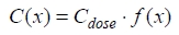
where Cdose is the implanted dose, C(x) is the concentrations as a function of the depth x, and
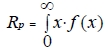
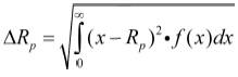
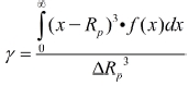
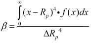
where the first moment Rp (projected average range) is the average range under normal implantation, the second moment ΔRp (standard deviation) represents the profile width, the third moment γ (skewness) indicates the asymmetry of the profile, and the fourth moment β (kurtosis) represents the extent of profile sharpness in the peak-concentration area. A gaussian profile has only two parameters due to symmetry, and the equation can be expressed as,
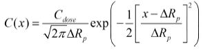
The projected average range (Rp) of the Gaussian profile is located near the peak concentration.
The equation of concentration distribution after annealing is due to diffusion effects. The Gaussian profile is generally not adequate to express asymmetry profiles caused for B, BF2 and dual (B and BF2) implanted silicon.
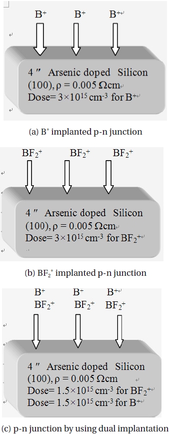
2. EXPERIMENTS OF B, BF2, AND DUAL IMPLANTATIONS
In this experiment, (100) arsenic-doped n type, silicon wafers with values with ρ of 0.005 Ω.cm, were used. The concentration of silicon substrate was about 1×1019 cm-3.
For the p type doping, B, BF2, dual (B and BF2) ions were implanted in silicon wafers. For the doping of source and drain formation for CMOS fabrication, three different implantations with the same doses were carried out into silicon substrate by using a VARIAN medium current implanter. Before the implantation, the accelerated energies were calculated by applying the massratio of elements for the same range. First, 15 keV 11B ions were implanted in silicon at 7℃ wafer tilt and a dose of 3.0×1015 cm-2. Second, 67 keV 49BF2 ions were implanted in silicon at 7° wafer tilt and a dose of 3.0×1015 cm-2. Third, dual (B and BF2) implantations were carried out. Namely, 67 keV 49BF2 ions were implanted in silicon at 7° wafer tilt and a dose of 1.5×1015 cm-2. Also, 15 keV B ions were implanted in silicon at 7° wafer tilt and a dose of 1.5×1015 cm-2. Three different implantations were carried out at 7° wafer tilt to avoid the channeling effect in Fig. 1.
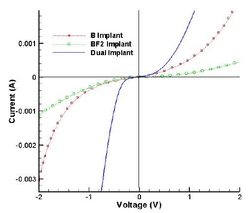
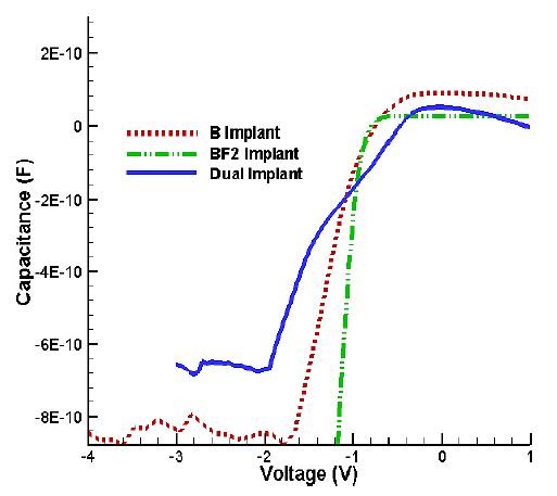
For the electrical activation, annealing processes with rapid thermal annealing (RTA) were carried out in a N2 gas ambient at 1,050℃ for 30 seconds. For the three implantation cases, the measured boron profiles were compared as depicted in Fig. 1. For the fabrication of three different diodes, the native oxides in implanted samples were etched off by dipping in a buffered oxide etchant (BOE) solution. After removal of the native oxide, the implanted wafers were coated with aluminum (Al) on the surface by using sputtering to form electrode material with thickness of 6,000Å. For the alloying process of good electrical contact, the implanted wafers were annealed in the 450℃ for 30 minutes under N2 ambient gas by using electrical furnace. The fabricated diode was scribed and cut off as a size of 5 mm × 5 mm by using a dicing saw. Current-voltage (I-V) and capacitance-voltage (C-V) characteristics of the diode were measured. The measured data of three different diodes are compared with one another in Figs. 12 and 13, respectively.
3.1 Comparisons with measured and simulated data
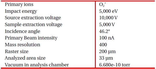
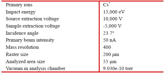
The profiles of implanted boron in silicon were measured by using SIMS. The experimental conditions for SIMS are shown in Table. 1.
The implanted profiles were measured by using CAMECA IMS 7f SIMS. The profile of boron implanted silicon is deeper than the other two cases. On the other side, the boron profile measured by using BF2 implantation in silicon is shallower than a direct B implantation, because 49BF22 is 4.46 times heavier than 11B and the range implanted of boron in 49BF22 is shorter than that of 11B. When 49BF22 is implanted, 11B+ and 38F2 + ions are dissociated and the range in 19F ions is deeper in the bulk silicon than in 11B because of the lower electronic stopping power of 19F. The profiles at the peak concentration have very similar shapes. Nevertheless, the profiles at the tail regions are different from the three implanted samples. This effect occurs because fluorine can trap interstitial silicon and cause the abnormal boron distribution from the interstitial silicon, defects, and vacancy distributions. For the explanation of amorphized layers with increasing implant doses, the defects dynamics were used citations from the published papers [15] instead of different experimental conditions, which were as follows. BF2 + ions were implanted with 50-keV energy at 0° into SiO2(200Å)/Si. The TEM (transmission electron micrograph) results of the specimens implanted with dose higher than 5 1014 cm-2 showed that the thickness of amorphized layers with increasing implant doses. The thickness of amorphized layers were measured to be 200, 400, and 550Å for the specimens implanted with 1 1015 cm-2, 5 1015 cm-2, and 1 1016 cm-2, respectively.
[Table 1.] Experimental conditions for SIMS measurements of 11B profiles.

Experimental conditions for SIMS measurements of 11B profiles.
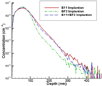
Boron ions were implanted in silicon at a 7o tilt angle to avoid channeling effects and the B profiles measured by using SIMS are shown in Fig. 2.
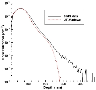
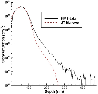
B ions were implanted in silicon at a 7° tilt angle to avoid channeling effects and the measured SIMS and UT-Marlowe simulation data are compared in Fig. 4. Although the avoidance of channeling effects are considered at a 7° tilting condition, the channeling effects is still shown in Figs. 3-5 from the SIMS data. The UT-Marlowe program can be used to verify implanted profiles in the crystalline silicon. The data of the UT-Marlowe simulation matches the SIMS data relatively well. For good statistical resolutions of profiles in crystalline silicon, 100,000 ions were selected for the UT-Marlowe simulation.
BF2 ions were implanted in silicon at a 7° tilt angle and compared between measured SIMS and UT-Marlowe simulation data in Fig. 4. The shape of the B profile is smaller than in other cases due to dissociation effects of B and F ions and fluorine can trap interstitial silicon.
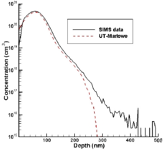
The dual (BF2 and B) ions were implanted in silicon at a 7° tilt angle for the boron profiles and compared between measured SIMS and UT-Marlowe simulation data in Fig. 5.
The implanted samples were annealed at 1050℃ for 30 seconds under N2 ambient gas by using RTA. After the annealing process at 1,050℃ for 30 seconds under N2 ambient gas, the boron profile in the BF2 implantation is shallower than in the corresponding boron profiles of B implantation because of retarded diffusion due to fluorine. The boron profiles of dual implantation shows the middle distribution between BF2 and B implantations except for peak concentration. The calculated data of implanted and annealed B are shown in Tables 2 and 3.
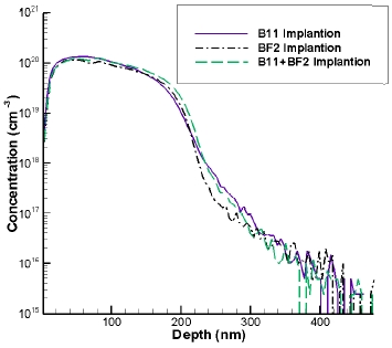
Implanted boron profiles were measured by using CAMECA IMS 7f SIMS and were compared with simulated data using the UT-Marlowe simulation tool. Three different implantations were carried out by using source ions of B, BF2, and dual (B and BF2). After the annealing process of the implanted samples at 1050℃ for 30 seconds in N2 gas by using RTA, the annealed boron profiles from SIMS are compared with one another in Fig. 6.
[Table 2.] The calculated B moments of SIMS and simulated data of UT-Marlowe program.
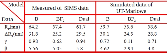
The calculated B moments of SIMS and simulated data of UT-Marlowe program.
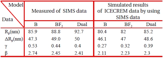
The calculated B moments of annealed SIMS and simulated data of ICECREM program after annealing.
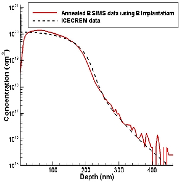
The peak concentrations are shown around 1.3 1020 cm-3 in Fig. 6. The measured SIMS data in Fig. 2 are simulated for the diffused profiles by using ICECREM in Fig. 7.
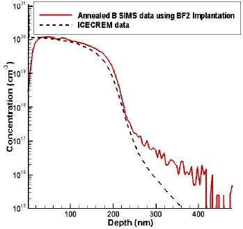
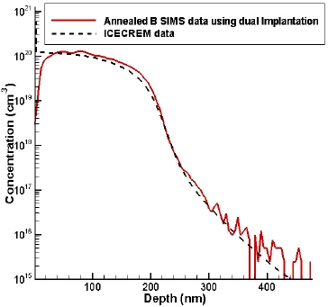
The peak concentrations are shown around 1.97 1020 cm-3 in Fig. 7. It can be explained because of different diffusion coefficients and a little bit of out-diffusion of boron toward the surface in real samples. In any case, the diffusion mechanisms show very similar results between Figs. 6 and 7. After the annealing process, the B profile implanted by using BF2 is shown as the shallowest profile due to the diffusion retarding effect of fluorine in Fig. 8. The profile of the dual implanted case is shown in the middle curve between the B and BF2 cases in Fig. 6. The annealed SIMS profiles are each compared with simulated data in Figs. 7- 9, respectively.
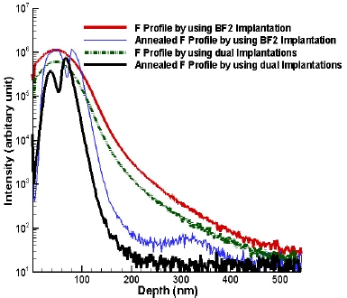
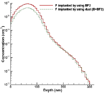
The implanted and annealed F profiles were measured using SIMS in Fig. 10.
The F profile implanted by using BF2 is shown as a solid line. On the other hand, the F profile implanted by using dual implantations is shown as a dash-dot-dot line, and has lower peak intensity due to a half dose of fluorine. The published TEM results showed that the dislocations have climbed towards the wafer surface as the length of anneal increased while F profiles reveal that 75% of implanted fluorine has out-diffused after 30 seconds RTA anneal at 1,100℃ [16]. Fluorine out-diffused but is trapped at residual implantation damage which consists of dislocation loops [16]. After the 30 seconds RTA anneal at 1,050℃, F profiles are measured by using SIMS. Two fluorine peaks are detected at the depth of 53.13 and 100.13 nm for BF2 implanted wafer and 35.34 and 67.06 nm for the dual implanted sample, respectively in Fig. 10.
In the experiments, F profiles reveal that 68.2% for the BF2 and 34% for the dual case of implanted fluorine have out-diffused after 30 seconds RTA anneal at 1,050℃. Because this result showed originally different fluorine dose ratio caused between the BF2 and the dual implantations.
[Table 4.] Experimental conditions for SIMS measurements of 19F profiles.
Experimental conditions for SIMS measurements of 19F profiles.
The measurement conditions for F profiles by using SIMS are shown in Table 4
The implanted fluorine profiles were measured by using SIMS in Fig. 10.
The simulated data from UT-Marlowe are shown in Fig. 11. The value of intensity of 106 in Fig. 10 corresponds to a concentration about 1021 in Fig. 11.The implanted F profiles are simulated by using UT-Marlowe tool in Fig. 11. The measured F profiles showed very similar forms to the simulated data, but the annealed F profiles are shown two peaks from the F behavior of fluorine diffusion from the bulk to surface because of saturation in the interstitial of silicon. The peak concentrations of the BF2 case are greater than those of the dual implantations due to a higher F dose.
The diffused F profiles could not be simulated due to trapping of interstitial silicon, and the movement of F from bulk to surface was not controllable for simulation because of different doses and diffused temperatures. After the annealing process, two peaks of the measured F have somewhat different forms between BF2 and dual implanted cases due to different doses. Up to now, the diffusion mechanism of F in silicon was not clearly explained, and there was not an accurate theoretical model from the published research papers. From the different temperatures, an explanation and model of the annealed F profile must be developed in the future.
3.2 Electrical measurements for the fabricated diodes
The measurements of current and voltage are shown in Figs. 12 and 13, respectively.
The diode fabricated using BF2 implantation has flat characteristics on the voltage axis. The diode fabricated using B implantation has steeper characteristics than the case of implanted BF2. The diode fabricated using dual implantations showed the best turn on voltage characteristics of the three different diodes. Namely, turn-on voltages were 0.39 V for dual, 0.6 V for B, and 0.67 V for BF2, respectively in Fig. 12. For the characteristic of breakdown voltages, the BF2 implanted case is relatively the best result from three p-n junction diodes fabricated by using different implantations.
The C-V characteristics of the three different diodes are measured and compared by using the HP C-V plotter. The C-V characteristic of the BF2 implanted diode changes rapidly from positive to negative voltage. From the three different diodes, the depletion layer in the BF2 case shows the fastest control from positive to negative voltage. The change of capacitance of the BF2 case is more abrupt than that of other cases. It means the depletion width of BF2 can be reacted faster than that of other cases from positive to negative voltage.
In the experiments, B, BF2, and dual (B and BF2) ions were implanted into n type silicon. For the electrical activation, the implanted wafers were annealed using RTA. The implanted and annealed SIMS profiles and the calculated range data were compared using UT-Marlowe and ICECREM simulation tools. They matched very well except channeling tail regions. The experimental results could be verified by the scaling of implanted ranges from different species and energies. For the formation of electrodes, the removal of native oxide was carried out using buffered oxide etchant (BOE) chemical treatments. Aluminums were coated onto the silicon by using sputtering technology. The implanted and annealed results show that concentration profiles for BF2 + implant are shallower than those for a single B+ and dual (B+ and BF2 +) implants in silicon. This effect was caused by the presence of fluorine, which traps interstitial silicon, and BF2 + implant have a lower diffusion effect than a single and dual implantation cases. The fabricated diodes were investigated for the electrical measurements of I-V and C-V. The electrical characteristics of VT (turn on voltage) using the dual implantations was the best result from among the three different diodes in Fig. 12. Therefore, the dual implantations for the formation of the P channel (P-MOS) can be used to improve the characteristics of the threshold voltage for the CMOS integrated circuits. The middle value of the C-V characteristics between B and BF2 implantations are shown in the dual implantation in Fig. 13. The change of capacitance of the BF2 case has a more abrupt shape than that of other cases. This means the depletion width of BF2 can be reacted more quickly than that of other cases from the operations of positive to negative voltage. After the BF2 and dual implantations, the SIMS profiles of F were matched very well with simulation data by using UT-Marlowe in Figs. 10 and 11. Nevertheless, the annealed F profiles showed two peaks and the diffusion mechanism was unexplainable and very complex for the trapping mechanism of interstitial silicon and out-diffusion toward the surface due to different temperatures.