Ever since the efficient and small molecular organic lightemitting diode (OLED) was reported for the first time by Tang and VanSlyke in 1987 [1], enormous interest has been shown in developing the emitting materials in order to realize highresolution full-color flat panel displays that can provide a long lifetime. However, the performance of blue emitting material is still not sufficient for their applications. There are very few reports of OLEDs with a deep blue color, high efficiency and a long operational lifetime [2-5].
Among the three principal colors necessary for display applications, or red, green and blue, blue-emitting materials and devices are particularly in need of improvement in terms of efficiency and color purity in comparison to green and red emitters. In recent years, developing a deep blue electroluminescence (EL) color with a CIEy coordinate value of 0.15 has been considered essential [6] because such emitters can effectively reduce the power consumption of a full-color OLED panel and can also be utilized to generate emission of other colors via energy transfer to a matching emissive dopant [2,7].
While high-efficiency green and red emitting colors can be readily obtained by doping the commonly used guest materials, such as tris(8-ydroxyquinolinato) aluminum(Alq3), a wider band gap host is essential for the efficient generation of a blue energygap host in order to obtain an efficient emission of blue dopant. Therefore, key technical issues for developing the deep blue OLEDs are not only finding the highly fluorescent deep blue dopant, but also appropriately matching the host material in order to enhance the probability of carrier recombination as well as the efficiency of Forster energy transfer from the host to the dopant molecule. There were a number of reports on the design and synthesis of dopants that are able to produce a deep blue photoluminescence [2]. However, due to the considerably blue-shifted absorption of these deep blue dopants, more suitable matching host materials, with sufficient spectral overlap for reasonably high Forster energy transfers, are needed in order to facilitate the generation of blue dopant emission with high efficiency, as well as the deep blue color [8].
Blue emission is undoubtedly a basic element in achieving a perfect white emission and there has been much effort focused upon exploring blue-emitting materials and improving color purity and efficiency of blue OLEDs [9-11]. Despite the fact that great progress has been made, much effort is still required to further improve the performance of the blue OLEDs, especially when considering efficiency, in order to meet the demands of display applications.
This work demonstrates deep blue OLEDs with a blue dopant of 4,4'-bis(9-ethyl-3-carbazovinylene)-1,1'-biphenyl (BCzVBi) within various host materials such as NPB, DPVBi and TPBi, and also discusses its two possible energy transfer mechanisms.
Indium tin oxide (ITO) coated glass was cleaned in an ultrasonic bath by a regular sequence, described as follows: in acetone, methanol, diluted water and isopropyl alcohol. Hereafter, precleaned ITO was treated by O2 plasma under the following conditions: 2 × 10⁻² torr, 125 W during 2 minutes [12]. Blue OLEDs were fabricated using high vacuum (1.0 × 10⁻⁷ torr) thermal evaporation and NPB, DPVBi, Alq3 and BCzVBi and Liq and Al were deposited by evaporation rates of 1.0, 0.1, 0.1, 5.0 A/s, respectively.
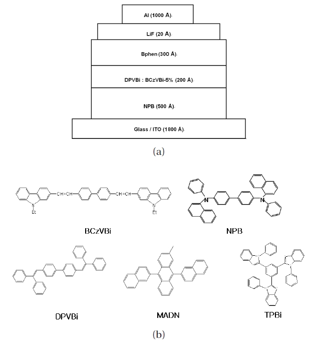
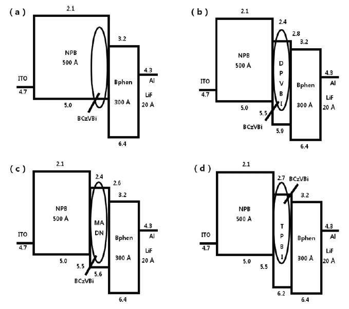
Figure 1(a) shows the schematic configuration of the blue OLEDs constructed within this study and Fig. 1(b) shows the molecular structures of the chromophores in the devices as emitting layer materials. The host-dopant layered blue OLED device structures, using blue fluorescence dopant BCzVBi with fluorescence host DPVBi, were as follows: ITO / N,N'-bis-(1- naphyl)-N,N'-diphenyl-1,1'-biphenyl-4,4'-diamine (NPB) as a hole transport layer / 4,4'-bis(9-ethyl-3-carbazovinylene)- 1,1'-biphenyl (BCzVBi) doped in 4,4'-bis(2,2'-diphenylyinyl)- 1,1'-biphenyl (DPVBi) as a blue emissive layer / 4,7-diphenyl- 1,10-phenanthroline (Bphen) as an electron transport layer / lithium fluoride (LiF) as an electron injection layer / aluminum (Al) as a cathode. Four different blue OLED devices were fabricated with a blue dopant of BCzVBi in combination with various host materials such as NPB, DPVBi, MADN and TPBi, respectively. With a varying direct current voltage bias, the optical and electrical properties of blue OLEDs such as current density, luminance, luminous efficiency, Commission Internationale de L'eclairage (CIExy) coordinates and electroluminescence characteristics were measured with a Keithley 236(Keithley Instruments Inc., Cleveland, OH, USA), LMSPR- 1000(Photo Research Inc., Chatsworth, CA, USA).
[Table 1.] Structures and characteristics of fabricated deep blue OLEDs.

Structures and characteristics of fabricated deep blue OLEDs.
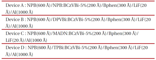
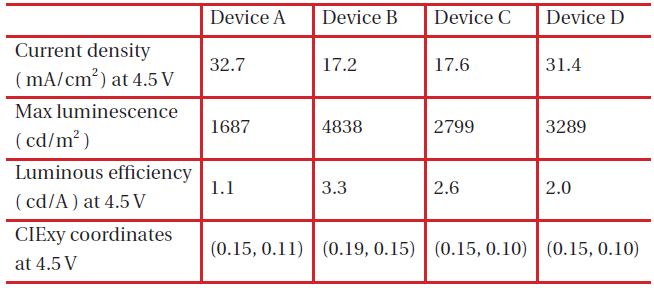
Device structures of various blue OLEDs are summarized in Table 1. Blue OLED devices of A, B, C and D are composed of NPB (500 A) / X : BCzVBi-5% (200 A) / Bphen (300 A) / LiF (20 A) / Al (1,000 A) with different host materials of X.
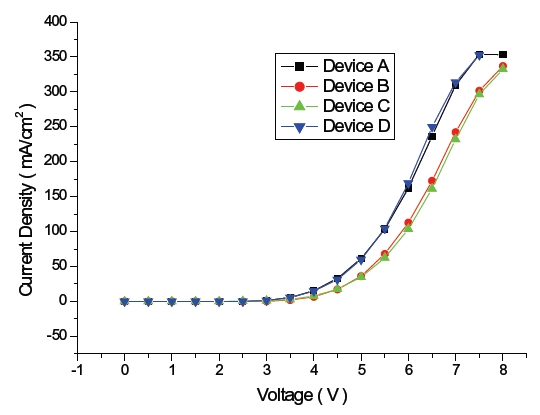
Figure 2 shows the current densities of blue OLEDs and those of device A and D were 32.7 and 31.4 mA/cm2 while those of device B and C were 17.2, 17.6 mA/cm2 at 4.5 V. This is due to the highest occupied molecular orbital (HOMO) energy level, 5.0 eV, of NPB and the lowest unoccupied molecular orbital (LUMO) energy level, 2.7 eV of TPBi, which is used to enhance the injections of both the hole and the electron from the hole transport layer and the electron transport layer, respectively, as described in the HOMO-LUMO energy diagram shown in Fig. 3.
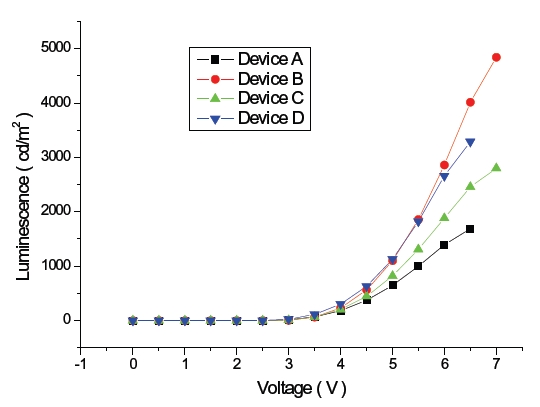
Figure 4 shows V-L characteristics of blue OLEDs and the maximum brightness of the devices B and D was 4,838 cd/m2 and 3,289 cd/m2 each, which is an improvement over device A with 1,687 cd/m2 due to the different hole-electron recombination probability in the emitting layer for each blue OLED. When considering energy levels of the hole transport material, electron transport material and host materials of emitting layer, HOMO energy levels of DPVBi and TPBi within device B and D are 5.9 eV and 6.2 eV, which are relatively high in comparison to 5.0 eV of NPB. However, LUMO energy levels of DPVBi and TPBi are 2.8 eV and 2.7 eV, which is relatively low in comparison to 3.2 eV of Bphen, which is an electron transport material. The energy gap of the HOMO level between DPVBi/TPBi and NPB is 0.9 eV and 1.2 eV, which is relatively larger than that occurring between MADN and NPB in order to decrease hole density within the emitting layer. On the other hand, the energy gap of the LUMO energy level between DPVBi/ TPBi and Bphen is 0.4 eV and 0.5 eV, which is relatively small in comparison to that between the MADN and Bphen in order to enhance the electron density within the emitting layer. According to the hole and electron mobility as well as the HOMO-LUMO energy band gap, the probability of hole-electron recombination within the emitting layer of the blue OLED devices B and D are relatively high in comparison to that of device C. Device A, including NPB as the hole transport material and host material of the emitting layer, shows the lowest brightness due to the largest LUMO energy gap of 0.9 eV from Bphen, and the electron transport layer resulted in less recombination for the hole and electron within the emitting layer.
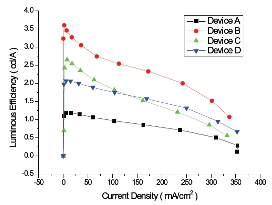
The luminous efficiency of blue OLED device B is 3.3 cd/A at 4.5 V, which is an improvement in comparison to those of device A, C and D which are 1.1, 2.6, 2.0 cd/A, respectively, as shown in Fig. 5. Device A has the largest LUMO energy gap of 1.1 eV, and between Bphen and NPB it is 1.1 eV, which makes it more difficult for electron injection from the electron transport layer to the emitting layer and then still being able to reach the lowest luminous efficiency. There are two different emission mechanisms possible within device B. Forster energy transfer will occur due to recombination of hole injection from DPVBi's HOMO and the electron injected from DPVBi's LUMO and then the exciton energy is transferred to BCzVBi. Also, the endothermic energy transfer between BCzVBi's LUMO and DPVBi's LUMO is done via the thermal excitation of accumulated electrons in LUMO of DPVBi via migration of holes in BCzVBi's HOMO levels. These two energy transfer mechanisms could also occur in device C and D with a different ratio. The energy gap of HOMO and LUMO between MADN and BCzVBi is 0.2 eV and 0.1 eV, each in device C, while between DPVBi and BCzVBi it is 0.4 eV and 0.4 eV, each for device B. Different energy gaps between the dopant and host materials can imply that the endothermic energy transfer in the emitting layer of device C will occur in less time when compared to device B in order to allow for a lower luminous efficiency. When comparing device B with device D for these energy transfer mechanisms, which effect the luminous efficiency, the energy gap of HOMO and LUMO between TPBi and BCzVBi within device D is 0.7 eV and 0.3 eV, which will enhance endothermic energy transfer better than device B, but a larger HOMO energy gap of 1.2 eV between NPB and TPBi, will suppress hole injection to the emitting layer and then eventually generate less Forster energy transfer. The luminous efficiency curves of device C also shows how Forster energy transfer dominates with a lower current density of less than 100 mA/cm2 while endothermic energy transfer does for a higher current density of greater than 100 mA/cm2. Thus, the energy transfer mechanism could be influenced by current density according to the energy gap between HOMO and LUMO of the hole transport, electron transport and host materials found in OLED devices.
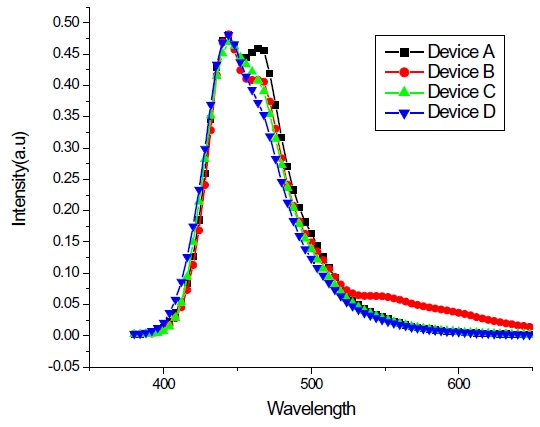
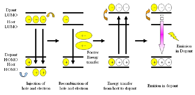
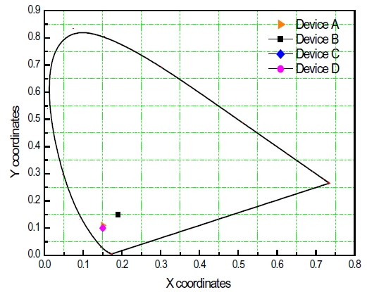
The electroluminescence (EL) spectra for blue OLED devices have two major peaks at 443 and 464 nm within the blue region caused by endothermic and Forster energy transfers, as shown in Fig. 6. Normalization, based upon the peak at 443 nm, helps the observation of different intensities from device A, B, C and D due to different HOMO-LUMO energy levels found within the host materials, which suggests that a Forster energy transfer might occur in a device order of A, C, B and D. When examining the intensity ratio of two peaks at 443 and 464 nm in the EL spectra, the blue OLED devices with a larger HOMO-LUMO energy gap between BCzVBi and the host material has a higher value for the sequence of D, B, C and A, which can be interpreted relative composition of Forster and endothermic energy transfer in blue OLEDs. Figure 7 depicts the possible energy transfer mechanisms for the blue OLED devices. Forster energy transfer occurs via hole-injection from the hole transport layer to the HOMO level of BCzVBi and recombines with the electrons of the LUMO level for BCzVBi later. Endothermic energy transfer renders that surplus electrons move to the LUMO level of BCzVBi and it shows a higher energy than the Forster energy transfer for the LUMO level in order to generate excitons. Table 2 summarizes key electrical and optical properties of blue OLEDs and Figure 8 shows the CIE coordinates for the blue OLEDs. Device B has a higher luminous efficiency of 3.3 cd/A with deep blue color coordinates of (0.19, 0.15) due to a perfectly balanced Forster and endothermic energy transfer.
[Table 2.] Electrical and optical properties of fabricated blue OLEDs.
Electrical and optical properties of fabricated blue OLEDs.
The blue OLEDs with different host materials and 5% of BCzVBi, as the blue dopant in the emitting layer, were prepared in order to observe the possible energy transfer mechanisms as well as the electrical and optical characteristics. The devices using NPB and TPBi as the host material maintain a current density that is twice as high in comparison to the other devices, with DPVBi and MADN at 4.5 V. Forster and endothermic energy transfers were considered as two possible mechanisms that could affect the efficiency of the blue OLEDs' luminousity. The electroluminescence spectra of the blue OLEDs include two major peaks at 443 and 464, which suggest that endothermic and Forster energy transfers occurred in the blue emitting layer. Device B, with DPVBi as the host material, achieves a deep blue CIExy with coordinates of (0.19, 0.15) and a higher luminous efficiency of 3.3 cd/A among the other blue OLED devices due to the optimum balance of two energy transfer mechanisms.