Silicon carbide is one of the most attractive and promising wide band-gap semiconductor materials with its excellent physical properties and huge potential for electronic applications. Up to now, the most successful method for the growth of large SiC crystals of high quality is the physical vapor transport (PVT) method [1,2]. Since further reduction of defect densities in larger crystal are needed for the true implementation of SiC devices, many researchers are focusing to improve the quality of SiC single crystals through the process modifications for SiC bulk growth or new material implementations [3-5]. It is well known that in order to get high quality SiC crystals, source materials with high purity must be used in the PVT method. Among the various source materials used in the PVT method, a SiC powder is considered to take an important role because it would directly influence the crystal quality of SiC crystals as well as the optimum temperature of single crystal growth, their growth rate and doping characteristics. In reality, the effect of powder on SiC crystal growth could definitely be exhibited the complicated correlation. Therefore, the present research was focused to investigate the quality difference of SiC crystals grown by conventional PVT method using various SiC powders.
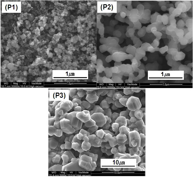
As shown in Fig. 1, we used three different SiC powders with different particles size (from 20 nm to 10 μm). These SiC source powders are named (P1) 20 nm, (P2) 0.1-0.2 μm, and (P3) 1-10 μm. According to specifications from the powder vender, the purity of powder (P1, P2) and powder (P3) were at least above 3N, 2N and 3N and the color of powder (P1, P2) and powder (P3) were dark green, bright green and yellow green with the naked eye, respectively. The particle shape of powder (P1, P2) appeared almost spherical and was of uniform distribution. The particle shape of powder (P3) also appeared spherical and the distribution of particle size was higher than powder (P1, P2). In this case, we focused more on how particle size affected growth rate. Consequently, we thought that the distribution of particle size would not significantly affect the result data.
The 6H-SiC crystals were grown on a (0001) Si-face by the PVT method and three different SiC powders were used as source materials. The SiC crystal was grown around 2,200-2,400℃ of the growth temperature and 30-50 mbar of argon pressure. The axial thermal gradient across the SiC crystal during growth is estimated in the range of 15-20℃/cm.
The image of the powder was evaluated using Quanta 200 field emission scanning electron microscopy before crystal growth, and the three PVT grown SiC crystals boules were sliced along the basal plane to produce a wafer and then polished using diamond paste in order to inspect the wafer surface with optical microscopy. To extensively analyze the crystals, X-ray patterns were analyzed for their identify polytype and the crystal quality of different SiC ingots using a high resolution XRD diffractometer (X'Pert-PRO MED, PANalytical, Holland). The chemical etch in molten KOH maintained at 450℃ for 10 minutes was used for defect observation with a polarizing microscope in the Nomarski mode. Electrical properties and absorption spectra of bulk SiC materials were analyzed by Hall measurement using van der Pauw geometry and a UV/VIS spectrophotometer, respectively.
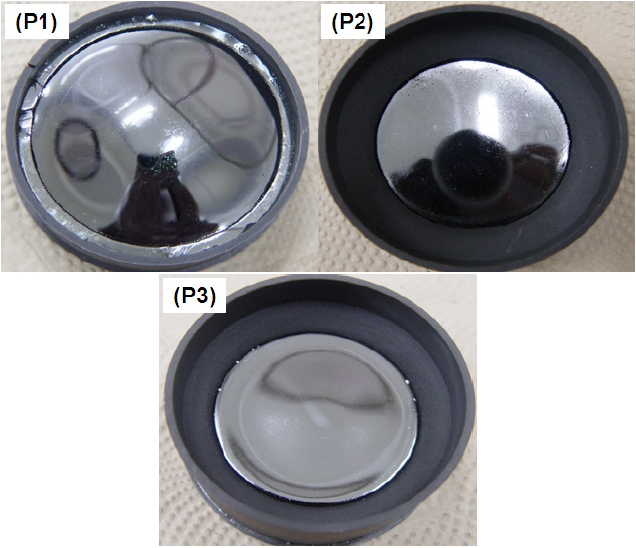
Optical photographs of three different crystal ingots are shown in Fig. 2. It is known that the growth rate depends on the particle size of the SiC source powder. The growth rate of bulk grown using SiC powder (P1) with a small particle size was higher than that using a larger particle size (P2, P3). The value of ingot (P1, P2) and ingot (P3) growth rate was 153 μm/h, 115 μm/h and 101.4 μm/h, respectively. The SiC powder also affected the top surface of SiC bulk grown using SiC powder (P1) was rather transparent. However, one grown by a larger particle size (P2, P3) was dark. This might relate to impurity incorporation with sublimation of the SiC powder. We are sure the sublimation speed of a small particle size (P1) was higher than a large particle size (P2, P3).
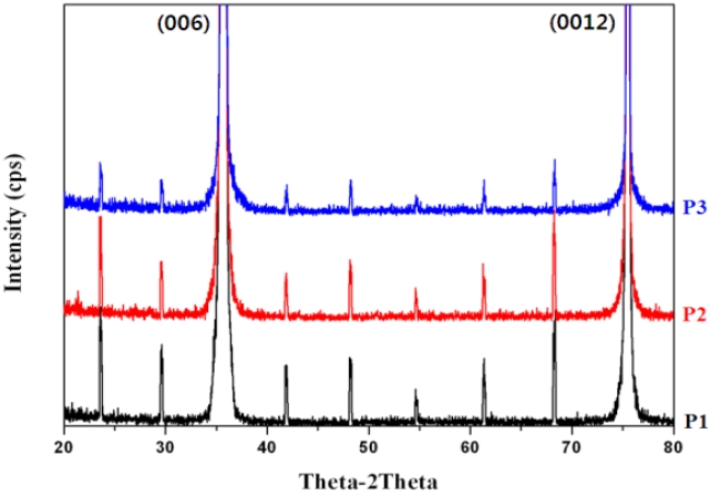
Figure 3 shows the diffraction patterns of wafer (P1, P2) and wafer (P3) measured with Cu K
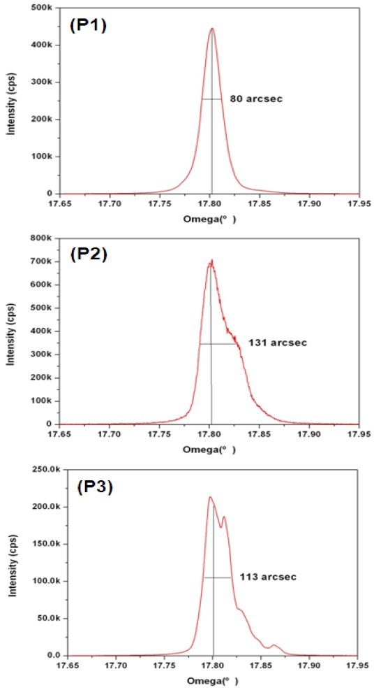
Figure 4 shows the full width at half maximum (FWHM) of (006) reflection in SiC wafers grown with various SiC powders. The FWHM values of all wafers were 80 arcsec, 131 arcsec and 113 arcsec, respectively. The wafer (P1) peak shape exhibited a very simple line. But, wafer (P2, P3) peak exhibited a slight mosaic distribution of crystals, which could relate to an existence tilted plane on crystals during crystal growth. The quality of a SiC single crystal grown using wafer (P1) was revealed to be better than that of crystals grown using wafer (P2, P3). No significant change in quality was observed in all SiC crystals, but quality of SiC single crystal grown using wafer(P1) was revealed to be slightly better than that of crystal grown using wafer(P2, P3).
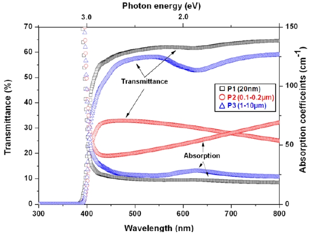
The absorption and transmittance spectra in the wavelength range from 300 to 800 nm in SiC crystals grown onto all three SiC wafers were shown in Fig. 5.
While the typical absorption spectrum of SiC crystals grown indicated that the SiC polytype with larger particle size (P2, P3) was the 6H-SiC with a fundamental energy absorption of about 3.04 eV, and the absorption spectrum of an SiC crystal grown with a small particle size (P1) exhibited a fundamental absorption indicating a bandgap energy of 3.05 eV. The typical transmittance of SiC was 60%. Wafer (P1, P2) transmittance indicated almost 60% and the SiC crystals indicated incorporation with nitrogen evidence near a photon energy of around 2.0 eV. However, the transmittance of wafer (P2) indicated around 35% and we could not observe evidence of nitrogen corporation. The included impurity of powder propagates incorporation with defect generation such as carbon inclusion and planer defect instead of SiC powder, and those defects then reduced the transmittance of wafer (P2).

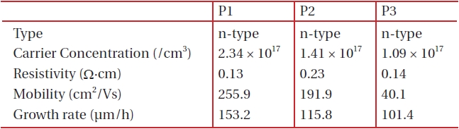
The electrical properties of an SiC single crystal grown with various SiC powders. (P1) 20 nm, (P2) 0.1-0.2 μm and (P3) 1-10 μm.
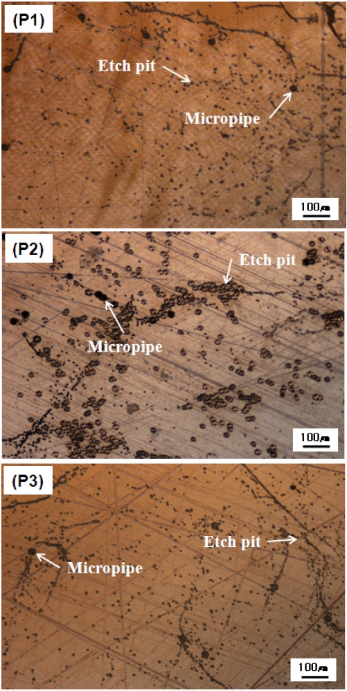
Figure 6 shows the surface morphologies of an SiC wafer grown with various powders and observed by an optical microscope in the Nomarski mode. A chemical etch in molten KOH maintained at 480℃ for 5 minutes was used for defect observation. The etched surfaces of all SiC wafers exhibited many shelllike etch pits and rounded etch pits, which are believed to be the basal plane dislocation intersecting the (0001) SiC surface and edge dislocations running parallel to the c-axis. It was observed that the distribution of defect density on etched surface (P1, P3) lower than etched surface (P2). The micropipe density of etched surface (P1, P2, and P3) were 30-35 ea/cm3, 65-75 ea/cm3 and 40- 50 ea/cm3, respectively.
Hall measurement was carried out for the wafers made from three different bulks as shown in Table 1. The carrier concentration of all wafers seems to be of the same order, but the mobility of the wafer made from powder (P1) was higher. The electrical properties of a SiC single crystal grown with powder (P1) was revealed to be better than that of a crystal grown with powder (P2, P3). Finally, we know that the smaller SiC powder (P1) produced a higher growth rate and higher mobility in sublimation bulk growth.
We investigate the quality difference of SiC crystals grown by the conventional PVT method using various SiC powders. The growth rate depends on the grain size of the SiC powder. The growth rate of bulk grown using SiC powder 20 nm with a small particle size was higher than that using a lager particle size (0.1- 0.2 μm, 1-10 μm). All three grown 2''-SiC single crystals were proven to be the polytype of 6H-SiC and powder of different sizes was not determined polytype inclusion. The crystal quality of an SiC single crystal grown using small particle (20 nm) was revealed to be slightly better than a larger particle size (0.1- 0.2 μm, 1-10 μm). The etched surfaces of a small particle size (20 nm) wafer exhibited a lower defect and micropipe density. The carrier concentration levels of about 1017/cm3 were determined from Hall measurements. The carrier concentration of all wafers seems to be of the same order, but the mobility of the wafer was higher made from powder (20 nm). It was revealed that the SiC particle size of SiC powder plays an important role in obtaining good quality, high growth rate and a reduction of growth temperature.