A great deal of research has been devoted to the p?type activation and defect nature of magnesium (Mg)?doped GaN epilayers because the p?type doping process is correlated to the low hole carrier concentration problem and issues with the mobility in p?type ohmic contact layers of optoelectronic devices [1]. It has been suggested that the Mg?H complex with an Mg acceptor can be compensated for by the role of hydrogen as a donor [2]. The incorporation of a hydrogen atom makes the thin film highly resistive so that there is no pathway for deriving holes in the quantum well active layer. Furthermore, due to the large approximately 260 meV binding energy of the Mg acceptor, only a small fraction of all electrically active Mg acceptors donate a hole at room temperature [3]. This behavior of a low solid solution is typical in wide band gap semiconductors and limits their application to optoelectronic devices [4], [5].
In order to overcome this problem, Mg delta?doped GaN thin films have been intensively investigated [6]?[8]. The delta doping process is effective in the enhancement of conduction and in the reduction of dislocation density due to growth interruption so that point?density distributions of both Mg and Si impurities can be localized for p?type and n?type GaN layers in thin films, respectively [6], [9]. This growth interruption causes the termination of the dislocation propagation and a change in the growth polarity. The reduction of impurity self?compensation and the enhancement of free carrier concentration are also achieved by delta doping [7]. It is desirable to investigate the defect structure of the delta?doped film compared to that of the uniformly doped film [8].
In this work, we investigated the defect structure of the Mg impurity center in the Mg delta doped sample using photoluminescence (PL) and electron paramagnetic resonance
(EPR) measurements. The delta?doped thin film shows a PL peak at 2.95 eV for both the as?grown and the post?annealed samples and results in a small Lande g?factor of 2.029 for the annealed sample.
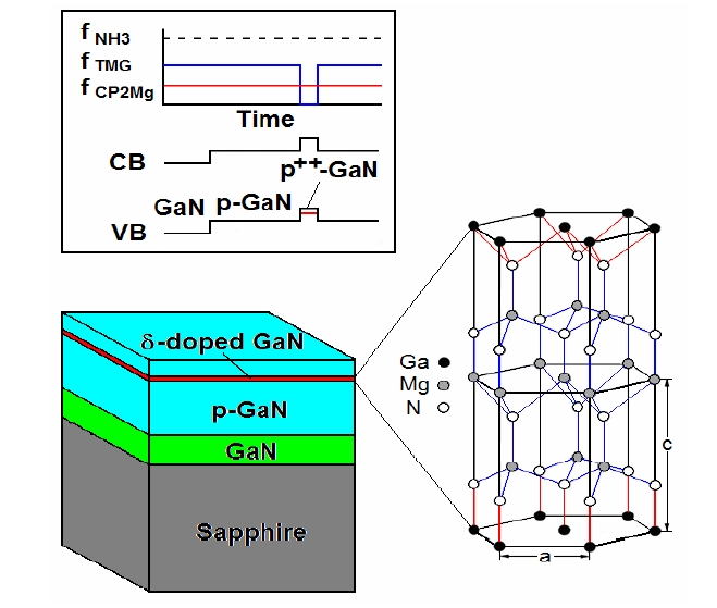
Figure 1 shows a schematic diagram of the heavily Mgdoped GaN epitaxial growth layer. During the heavy Mg doping process, an inclusion of the Mg delta?doped layer was carried out by interrupting the flow rate of the trimethylgallium (TMGa) source. The sapphire substrate was cleaned with an acetone solution after the surface was etched by a mixed solution of H3PO4 and H2SO4. The substrate was thermally etched in a hydrogen ambient at 1,100℃ in a metal?organic chemical vapor deposition (MOCVD) reactor for 10 min. prior to the formation of the nucleation layer at the substrate surface. Nitridation was carried out by supplying H2 with preheated NH3 gas. As shown in Fig. 1, a 30?nm thick nucleation layer was introduced, at a low temperature of 520℃, for geometrical bonding at the sapphire surface due to the large lattice mismatch between the sapphire substrate and the GaN film. Then, high?temperature epitaxial growths of uniformly Mg?doped GaN films with a thickness of 0.2 μm at 1,100℃ were performed by adding the Mg doping source of Cp2Mg into the main stream of hydrogen, ammonia, and TMGa.
In addition to this regular Mg doping, the Mg delta?doping via an instantaneous termination of the TMGa source was performed near the surface of the GaN film. We grew two samples with a uniformly Mg?doped GaN layer (uniform double layer [UDL] sample) with a thickness of 0.2 μm and a uniformly Mg?doped GaN layer with the same thickness and the inclusion of an Mg delta?doped layer (UDL/diffuse double layer [DDL] sample) via growth interruption near the surface. These two types of Mg?doped films were thermally annealed
in a vacuum chamber at a temperature of 850℃ for 20 min. The Hall effect measurement for the annealed sample of the uniformly doped thin film showed a carrier concentration and hole mobility of 2.58 × 10¹⁷/cm3 and 10 cm2/V?sec, respectively.
The EPR measurement was performed in a Bruker 300 ESP X?band (9.5 GHz) spectrometer equipped with a liquid?helium flow cryostat at a temperature of 4 K. The background EPR signals due to the sapphire substrate were separated from the thin film signals of the acceptor lines. Room?temperature PL measurements were performed on each sample at 325 nm of a He?Cd laser for excitation.
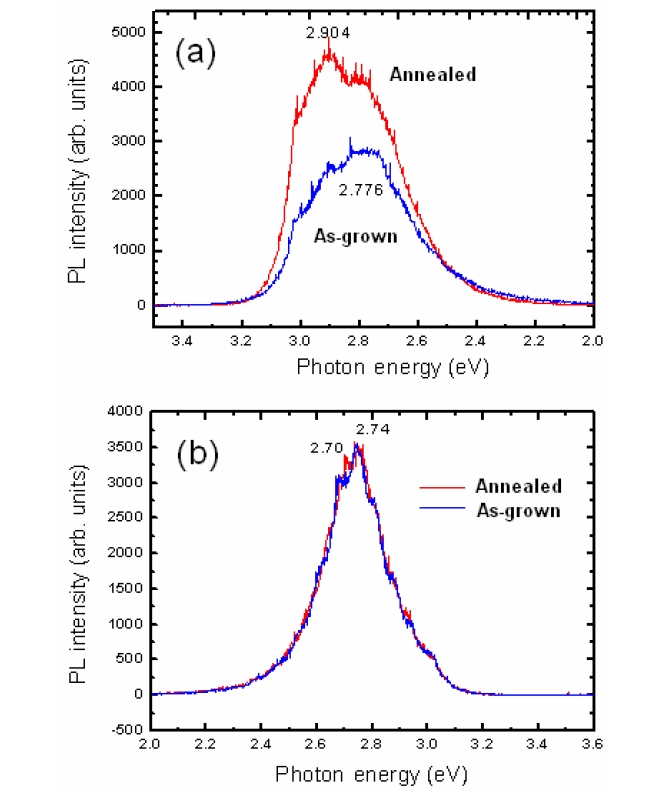
Figure 2 shows the room?temperature PL spectra from both the UDL and UDL/DDL samples. The as?grown UDL sample shown in Fig. 2(a) displays the typical blue emission peak at 2.776 eV, which is correlated with a relatively low concentration of Mg doping. This is attributed to a transition from the conduction band to a deep level of an Mg acceptor about 0.5?0.55 eV above the valence band [10]. When annealed at a temperature of 850℃, the UDL sample showed an enhanced PL intensity with an extra PL peak at 2.904 eV, indicating a typical PL band for the heavily doped GaN sample [11]. For the room?temperature PL spectra from the UDL/DDL sample shown in Fig. 2(b), the as?grown UDL/DDL sample shows the
PL peak at 2.74 eV. This results from the uniformly doped layer, as was seen with the as?grown UDL sample. However, the annealed UDL/DDL sample shows the same PL peak location, but the intensity is decreased.
The annealing effect at the temperature of 850℃ enhanced the PL intensity by increasing the PL centers for the regularly doped UDL sample, but it was not effective in increasing the PL centers from the delta?doped UDL/DDL sample. During the delta?doping process at high temperature, 1,050℃, the atomic bonding structure of the delta?doped layer was modified and changed the growth conditions. The N species can be expelled from the potential barrier in the growth mechanism via introduction of the Mg species in the delta?doping process. This may also imply a strong reduction in the Ga vacancies, and the changed growth conditions enhanced the formation of N vacancies, resulting in a quench effect on the PL centers. The PL quenching is influenced by the negative electron affinity due to strong atomic bonds in the UDL/DDL sample [12].
For the heavily Mg?doped GaN sample, several defect models were suggested such as interstitial Mg incorporated with nitrogen vacancies (MgI?VN) under the Ga?rich ambient [13] and Ga?substitutive Mg atoms incorporated with N?vacancies (MgGa?VN) under the N?rich ambient [14]. As the annealing process is applied, the hydrogen does not form a bond with the Mg atoms but prefers the anti?bonding site of one of the N neighbors, resulting in the formation of N?H bonds [14], [15]. The H atoms donate electrons to the Mg acceptor level
and form p?like orbitals located on the N atoms surrounding the Mg acceptor. The highest charge density at the bonding center includes unpaired electrons very close to N, and the anti?bonding site of N forms a bond with H. Therefore, in the delta?doped layer, the hole?bound Mg?N atomic structure can be established. Study on the magnetic field dependency of PL centers has previously been carried out.
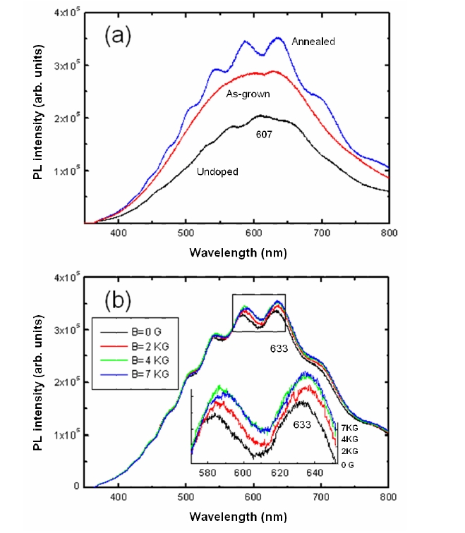
Figure 3 shows the magnetic field dependence of the PL spectra. Under a magnetic field of 4 KG in Fig. 3(a), the undoped sample shows a peak at 607 nm that is strongly related to the dislocation defect?induced PL. The as?grown UDL/DDL sample shows an enhanced intensity, and the annealed sample shows further enhancement. The annealed sample also shows a strong oscillation at the surface, indicating Fabry?Perot interference of the GaN thin film. For the annealed UDL/DDL sample shown in Fig. 3(b), the magnetic field effect on the PL intensity is very small, but the peaks can be red?shifted as the magnetic field is increased. Without the magnetic field, the UDL/DDL sample shows a PL peak at 632.5 nm, and as the magnetic field increases to 2, 4, and 7 KG, the peak shifted to 634.4, 635.1, and 636 nm, respectively.
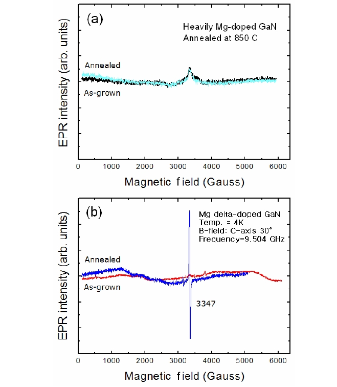
Figure 4 shows the EPR spectra for both the UDL and UDL/DDL samples. The regularly doped UDL sample in Fig. 4(a) shows no EPR spectra for either the as?grown or the annealed samples. This indicates that the as?grown UDL sam
ple provides no unpaired electrons during the formation of the Mg?N?H complexes, and especially, the annealed UDL sample with the thin film thickness of 0.2 μm did not provide sufficient hole spin density to show a signal in our experimental setup. However, Park reported a sharp EPR spectrum from the UDL/DDL sample [16], as shown in Fig. 4(b). The EPR spectrum appears in the annealed sample, but not in the asgrown sample. The observed EPR spectra is very sharp and narrow, indicating that the spin density is very large and similar to the defect signal from the bulk semiconductor material due to the delta doping process.
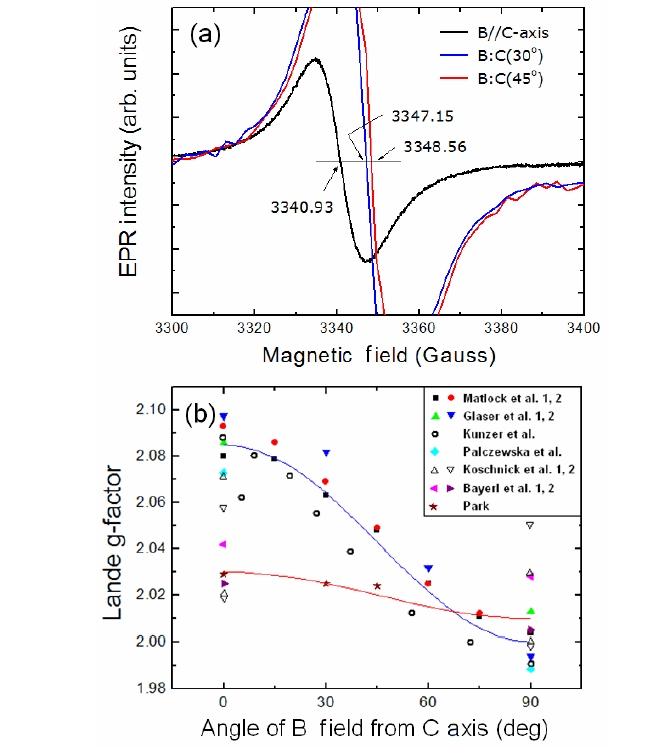
For angular variation in the EPR resonance [16], the Mg delta? doped sample in Fig. 5(a) shows a sharp Lorentian resonance line observed at B=3347.1 G at an angle of 30° from the normal direction of C(0001) plane with a full width at half maximum (FWHM) of 17.3 G. The microwave frequency for resonance is about 9.504 GHz for the measurement at an angle of 30°. The resonant position of the applied magnetic field has the following relationship: B0=hν/g(θ)μB and g(θ)=(g∥ 2cos2θ+g┴ 2sin2θ)1/2, where ν is the resonance frequency, μB is the Bohr magneton (9.2749×10?28 J/G), h is the Planck constant (6.6261×10?34 J?s), g(θ) is the Lande g?factor corresponding to the angle θ of the magnetic field B0 from the c?axis. The derived g?value is g(30°)=2.026(1). Fig. 5(a) shows the very slight anisotropic behavior of the EPR signals. For the microwave resonance frequencies of 9.502, 9.504, and 9.491 GHz, the g?values at 0°, 30° and 45° are obtained as 2.029(5), 2.026(1) and 2.022(5) with FWHMs of about 13.2, 17.3, and 18.1 G, respectively. The derivative g?value at the right angle is about g┴=2.014(5). This g?value is still larger than that of a free electron, ge=2.0023, as expected for most free acceptors. The intense signal at an angle of around 30? 45° is consistent with the axis of the Mg?N bond line [17].
The uniformly doped thick films have been known to yield very broad EPR signals [18]?[20]. As shown in Fig. 5(b), these films showed relatively large g?values around g∥=2.09?2.10. Because of the low hole carrier concentration in the Mgdoped GaN thin film, a very weak EPR signal from the unpaired dangling bonds has been observed for g∥ values of 2.10 [18]. Optically detected magnetic resonance has revealed several Mg?related recombination centers with reported gvalues of g∥=2.08 and g┴ =2.00 for uniformly Mg?doped GaN sam ples. The uniformly doped samples with a PL band peaked around 2.79 eV and also revealed an EPR signal with large values of g∥=2.073?2.112 with an FWHM of about 140 G [19]?[21]. The thick epitaxial films have the resonance behavior with weak intensity with a broad FWHM due to the limited solid solution of Mg dopants.
According to Koschnick et al. [22], an Mg?doped sample shows a PL?EPR resonance with g∥=2.07, g┴=2.03 having a broad PL at 2.74 eV, and the highly resistive sample showed a PL?EPR resonance with g∥=2.057, g┴=2.045 having broad PL at 3.12 eV. The PL?EPR resonance of g∥=2.07, g┴=2.03 in this study was similar to those observed by Glaser et al. [19] and Kunzer et al. [20] and that assigned to a deep Mg?related complex. There is another report on relatively small values, g∥=2.025?2.042 and g┴=2.005?2.028 with a FWHM of about 150 G, in electrically detected magnetic resonance [23]. This indicates that the Mg?doped samples can be classified into two groups based on their large or small g?values.
A large g factor represents the defect properties of a broad EPR spectrum with large PL centers for the (MgGa?VN) defect complex. The EPR signal was quenched at the high annealing temperature of 850℃. The delta?doped g?values were assigned to the small value group, although there was a large difference in the FWHMs. The very small FWHMs of the EPR spectra signal from the delta?doped layer were similar to the signal in the bulk material, rather than that of the epitaxial film. The EPR signal was very strong even at an annealing temperature of 850℃. However, the defect center did not reserve PL centers.
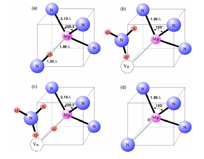
This delta?doping effect can be speculated from the atomic structure of the defect site in the crystal, as shown in Fig. 6. For the heavily doped UDL sample, the as?grown sample formed a defect site with the cooperation of hydrogen bonds as shown in Fig. 6(a). The annealed UDL sample formed the MgGa?VN complex with the NH3 molecular species over a range of annealing temperatures from 600 to 850℃ as shown in Fig. 6(b). For temperatures higher than 850℃, the NH3 molecular species can diffuse from the substance. This defect site forms the PL center with both the MgGa?acceptor and the VN?donor [24]. However, the hole density of the defect site is very broad and shows a large EPR signal and a broad PL spectra, indicating the potential fluctuation.
For the delta?doped UDL/DDL sample, the as?grown sample formed a defect site with a nitrogen vacancy, which was saturated by a hydrogen bond and interstitial molecules as
shown in Fig. 6(c). The hydrogen saturated defect site showed no EPR signal, but the PL centers were still active. For the annealing process at a temperature of 850℃, the defect site formed nitrogen antibonding with the dissociation of hydrogen gas as shown in Fig. 6(d). This defect site showed a hole center from the EPR signal, and the no donor site had no PL centers. For a monolayer of Mg atoms in the GaN thin film, the atomic density was 6.81 × 10¹⁵/cm2 and a sufficient electron spin density was provided by the Mg dangling bonds, which yielded a relatively sharp EPR peak. The Mg delta?doping process cannot enhance the PL centers but is useful for the formation of a hole channel in the Ohmic metal contact area.
In summary, the delta?doping effect on Mg?doped GaN thin film was investigated in terms of the PL and EPR characteristics. The as-grown UDL/DDL sample showed PL bands peaked at 2.74 eV, identical to the annealed sample. The as-grown sample also showed either the same or lower PL intensity as that of the annealed sample after the post-thermal annealing process. Therefore, the delta?doping was not effective in enhancing the PL centers. Furthermore, the EPR signal from the annealed UDL/DDL sample resulted in a relatively small g factor of g∥=2.029 compared to the literature values of about g∥=2.09 from relatively thick and uniformly Mg-doped GaN films. This implied that the defect mechanism of the delta-doped layer was totally different from that of the regularly doped layer. This difference may be due to the deep hole center of the Mg-N atomic structure rather than from a defect structure of the MgGa-VN complex. The delta?doping process will be useful for hole channel transport on p-type GaN surfaces attempting to contact ohmic metal.


![The electron paramagnetic resonance (EPR) signals for boththe regularly Mg?doped UDL sample and the Mg delta?doped uniform/diffuse double layer (UDL/DDL) samples at low temperature, 4K. The annealed delta?doped UDL/DDL sample shows EPR resonance.The as?grown Mg delta?doped GaN film does not show the EPR signal,and the heavily Mg?doped GaN films for both the as?grown andannealed UDL samples do not show EPR signals due to the low spindensity at a thickness of 0.2 μm [16].](http://oak.go.kr/repository/journal/10142/E1TEAO_2010_v11n1_37_f004.jpg)
![The electron paramagnetic resonance (EPR) signals for various directional orientations measured from the annealed Mg deltadoped thin film at low temperature, 4 K [16], and various Lande gfactors of Mg dangling bonds in GaN as a function of the angle between the magnetic field and the c axis. The data were classified into two groups indicating two types of deep hole centers.](http://oak.go.kr/repository/journal/10142/E1TEAO_2010_v11n1_37_f005.jpg)