Currently the surface treatment methods used to enable solar cells to collect light effectively include surface texturing and antireflection film formation [1], [2]. The antireflection film formation method, which can be carried out more simply than the surface texturing method, applies to almost all solar cells, now. Applying a antireflection film on the surface of a solar cell reduces the reflectance to less than three layers [3]. In general, the more layers of antireflection film coated on the materials with an appropriate refractive index ratio, the wider the wavelength range in which it can get a lower reflectance [4]?[6]. However, usually less than three layers are used in order to meet both price competitiveness and productivity rates. A single layered structure may effectively reduce the reflectance if it is manufactured side by side with surface texturing, however the wavelength range in which it can get low reflectance is narrow, which is not effective.
Recently, silicon nitride films, which contain hydrogen acting as surface passivation, and antireflection films have been used [7]. Currently the methods of forming antireflection films include vacuum evaporation, chemical vapor deposition, spin coating, screen printing, spray coating, etc. This experiment tries to manufacture a single?layered MgF2 structure in order to produce a antireflection film that is competitive in price and has a simpler process [8], [9].
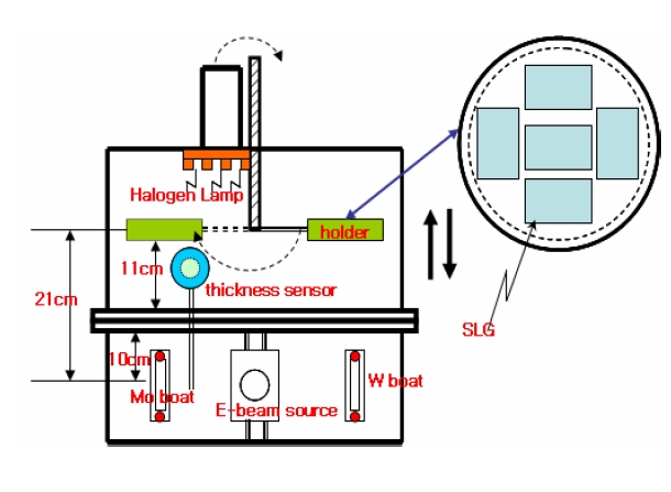
Korea Vacuum's KV?660 (10?7 torr), seen in Fig. 1, was used as the thermal evaporator used for the manufacturing of a MgF2 thin film. Its board could be heated using a halogen lamp and a thickness monitor (XTC; InFicon Inc., New York, USA) was incorporated with it for measuring the thickness of the thin film [10]. MgF2 has a high penetration ratio in a wide wavelength range from the 120 nm ultraviolet ray in a vacuum to the 900 nm infrared ray. It is a material with a low refractive index in the visible spectrum, and is mostly used for non?reflective coatings and as a protective layer because of its high durability.
It has been reported that non?reflective coatings increasesthe penetration ratio for unabsorbed thin films and the efficiencyof solar cells by reducing the reflectance. Antireflectionfilm can be an accurate non?reflective coating only if theoptical thickness of film is at a 1/4 wavelength of the incident
rays. This usually requires a two?layer film to decrease the reflectance and reduce the thickness difference found in a single layer. However, for this paper we decided to apply the MgF2 deposition only.
This was done because of its relatively simple manufacturing process and low price which could contribute to broad practical use of solar cells, and also for the application to optical devices other than solar cells which require a low reflectance. The manufactured MgF2 antireflection film was deposited at voltages between 1.20 v and 1.60 v. Cerac Corporation's 99.99% pure, 1?3 mm pcs type MgF2 material was used. This experiment mainly investigated the factors dependant on the substrate temperature and the deposition thickness. We dried the soda lime glass using acetone and distilled water after ultrasonic cleaning one by one and then installed them on a holder.
3.1 The structure properties of the MgF2 thin films
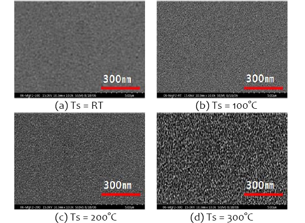
Figure 2 is an electron microscopic picture of when the temperature of the MgF2 board was changed from room temperature to 300°C.
As seen in the picture, the higher the temperature of the heat treatment is, the greater the grain size, and in the RT, a small pin hole was observed at 100°C. The condition of the surface of the thin film got much better at a substrate temperature of 200°C. However it was observed that the surface of the MgF2 thin film got rougher at 300°C.
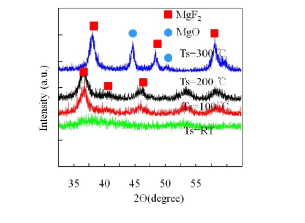
Figure 3 shows the X?ray diffraction result of the MgF2 film at each substrate temperature. One can see that as the substrate temperature increases, the strength of peak gradually increases, while the range of the peak gradually decreases. It appears that the MgF2 was crystallized and a diffraction peak appeared in the MgO as the temperature of the heat treatment increased. The MgO was generated by the oxidation of the MgF2.
3.2 The optical properties of the MgF2 thin films
The MgF2 film was coated using heat treatment methods
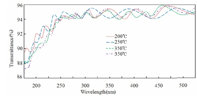
with deposition at different substrate temperatures. The penetration ratio of the film was measured using a spectrophotometer. Fig. 4 shows the spectrum of the penetration ratios of the MgF2 antireflection film as the substrate temperature changes.
It was found that the penetration ratio of the film whichwas developed at a substrate temperature of over 250°C decreased.The results of the measurement of the refractive
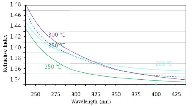
index with an optical laser?induced deposition is shown in Fig. 5 in which one can see that the refractive index increases at a substrate temperature of over 250°C .
It may be analyzed that this is the result of the faster molecularmotions occurring at higher temperatures Consequentlythe finer the thin film is the higher the refractive indexgets.
Meanwhile, at the substrate temperature of 200°C, the penetration ratio and the refractive index differ from the results found at the other substrate temperatures, in other words, the refractive index of the thin film developed at 200°C is higher than those developed at 250°C and 350°C. At the low temperature of 200°C, the MgF2 film partially crystallized and yet remains amorphous, so the grain boundaries blur while a few get in?between the boarders. As a result, the coating of the thin film gets finer and the refractive index gets higher.
3.3 The antireflection film properties of the MgF2 thin films
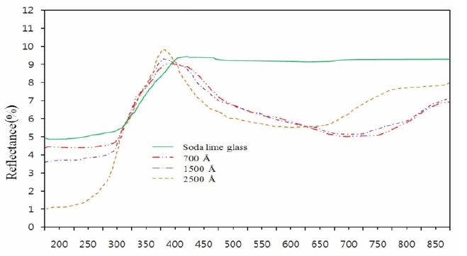
Figure 6 shows the changes of the reflectance according to the deposition thickness of the antireflection film. You can see that the reflectance of the soda?lime glass before the formation of the antireflection film is approximately 9.5% while the reflectance of the deposited MgF2 antireflection film with the thickness of 700?1,500 A is approximately 5%, which is lower than the one with the thickness of 2,500 A.
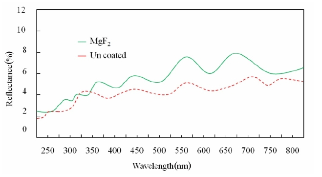
Fig. 7 is a comparison of the surface reflectance after the completion of the Mo/CuInS2/CuGaS2 layer with that measured after the deposition of the MgF2, in which one can see that the reflectance of the solar cell before the antireflection film formation was approximately 3.5% while after the formation decreased to approximately 2.5%.
The MgF2, manufactured with electron beam evaporation method, has a high penetration ratio in vacuum ultraviolet with a broad wavelength range from 120 nm to 900 nm. It is a material with a low refractive index in the visible spectrum which is mostly used for non?reflective coatings. It can do an accurate non?reflective coating only if the optical thickness is a 1/4 wavelength of the incident rays and usually consists of a two?layer film to decrease the reflectance more and reduce the thickness difference of a single layer. In this paper, we deposited a manufactured antireflection film at the conditions of 1.20?1.60 v to deposit only MgF2. The characteristics of the thin film obtained at a substrate temperature of 200°C is confirmed to be the best, while the reflectance was improved approximately 4%. As a result of the comparison between the pre?coating and post?coating reflectance of the thin MgF2 films, the reflectance before the antireflection film formation was 3.5% while that after the formation decreased to 2.5%.