Recently, radio frequency identification (RFID) technology has become a key component in manufacturing, distribution industries, and banking services [1]?[3]. Mobile RFID is widely used at the high frequency of 13.56 MHz, and in the ultra?high frequency band from 860 to 960 MHz. The mobile RFIDs that use the 13.56 MHz carrier frequency are limited to near field communication, however this limitation is very useful in the protection of privacy and in personal authentication processes. These mobile RFIDs, using the ISO 14443 type A standard, use 100% amplitude shift keying (ASK) modulation to create a "pause" period. A normal clock recovery circuit has a difficulty in recovering the clock during the pause period. It should be noted that the ISO 14443 type A and type B methods have different modulation index values, 100% and 10%, respectively [1].
We propose a new circuit structure for an RFID transponder analog front end (AFE) which easily recovers the clock of a 100% modulated ASK signal using the ISO 14443 type A standard. A digital phase locked loop (DPLL) incorporating a charge pump enable circuit is used to recover the clock of a 100% modulated ASK signal during the pause period. We also used a high voltage lateral double diffused metal?oxide semiconductor transistor (LDMOST) [4] for the rectifier and clock recovery circuit of the DPLL at the point where the high input signal is directly applied. The proposed RFID transponder AFE was verified by circuit simulations and the measurements of a fabricated chip manufactured using the 0.18 ㎛ complementary MOS (CMOS) standard process.
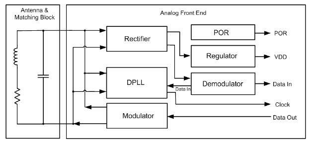
The RFID system consists of a reader with a computer network and an RFID tag which has an antenna, an AFE, and a digital control block. A conventional AFE block consists of a rectifier, a modulator, a demodulator, a regulator, a clock generator, and a power on reset (POR) section. This circuit can recover the clock of a 10% modulated ASK signal, but has difficulty in recovering the clock of a 100% modulated ASK signal during the pause period. To overcome this problem, we propose a new circuit block for the AFE, as shown in Fig. 1. The proposed AFE circuit has a dynamically enabled DPLL instead of the clock generator used in the conventional AFE. This DPLL can recover the clock of a 100% modulated ASK signal during the pause period.
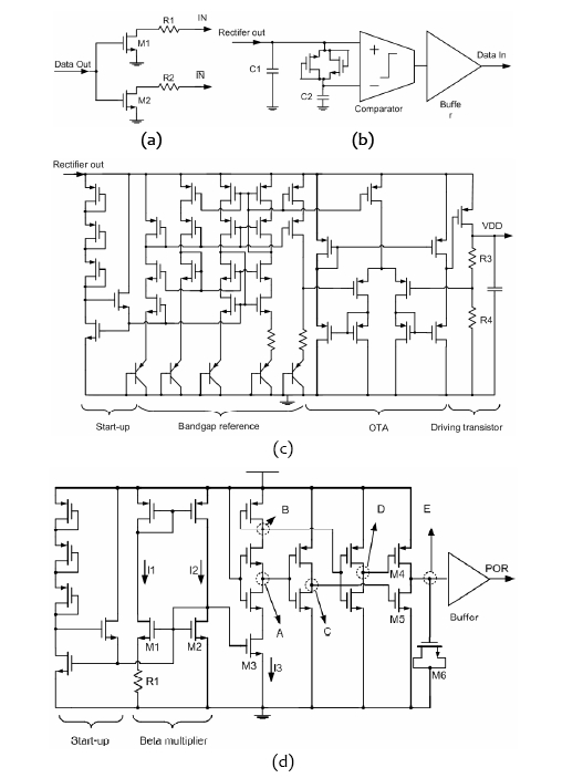
The modulator, as shown in Fig. 2(a), is used to change the amplitude of the LC resonant tank according to the output data. The output data signal from the digital control block shown in Fig. 1 is applied to the modulator, which changes the impedance of the LC resonant tank. We used a resistive load modulation technique, which utilizes the load resistors connected in series with the drain of the modulator switch transistors [5]. Depending on the output data, the modulator output resistance and thus the Q factor of the parallel LC resonant tank are varied to modulate the amplitude of the LC tank.
The demodulator, as shown in Fig. 2(b), recovers the information from the incoming signal. The output signal from the rectifier is applied to the demodulator whose output is transferred into the digital control block. The demodulator consists of a diode?connected metal?oxide semiconductor field?effect transistor (MOSFET) pair, capacitors and an operational transconductance amplifier (OTA) comparator [3], [6]. The rectifier output signal is applied to the diodeconnected MOSFET pair to obtain the average input signal. The envelope of the input signal is compared to the average level and then amplified.
The regulator, as shown in Fig. 2(c), is used to make the supply voltage independent of the incoming signal strength and the temperature. The regulator consists of a band?gap reference circuit utilizing a parasitic bipolar junction transistor (BJT) in the standard CMOS process, a start?up circuit, and an OTA with a driving transistor. A wide swing cascode mirror structure was adopted to increase the output voltage range in the band?gap reference circuit [7].
The POR, as shown in Fig. 2(d), is used to generate a reset signal to the digital control block during the initial supply voltage stabilization stage. The POR circuit consists of a startup circuit, a beta?multiplier reference, and a circuit to create a reset signal [2], [8]. When the RFID power supply increases, MOSFETs M1, M2, and M3 start to have current flow. As a result, the voltages of nodes A and B rise up, but the voltages of nodes C and D fall down. MOSFET M4 conducts more current than M5 and thus the node E voltage ramps up until the regulator output reaches the threshold voltage of the POR.
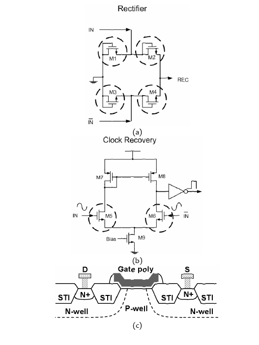
2.2 The LDMOSTs for the rectifier and clock recovery circuit
In the rectifier and the clock recovery circuit of the DPLL, where the high voltage input signal is directly applied, we used a specially designed high voltage LDMOST, as shown in Fig. 3 [4]. This LDMOST was designed using the standard CMOS process, and the lightly doped n?well layer plays the role of a drift region, which can reduce the drain electric field. The channel length and the electrical gate oxide thickness are about 3 ㎛ and 7.2 nm, respectively. The full wave rectifier is a bridge composed of LDMOSTs. LDMOSTs can operate at high voltages, but have smaller current driving capabilities, so
we used a parallel?connected LDMOST in the rectifier in order to support enough current. The measured breakdown voltage of the LDMOST was 14.3 V. Note that the breakdown voltage of the conventional MOSFET used in the 0.18 ㎛ standard CMOS process is 4.6 V.
2.3 The DPLL with a charge pump enable circuit
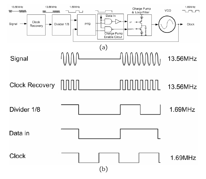
The DPLL, shown in Fig. 4(a), consists of a clock recovery circuit, a divider, a phase frequency detector (PFD), a charge pump enable circuit, a charge pump, a loop filter, and a voltage controlled oscillator (VCO) [7]. The input clock signal of 13.56 MHz is recovered by the clock recovery circuit, which is divided down to 1.695 MHz by the divider. This signal is then compared with the VCO output signal in the PFD. The charge pump is activated by the charge pump enable circuit, dependant on the demodulator output. The error signal of the PFD is then smoothed out by the charge pump and the loop filter. This output signal goes to the VCO and is used to correct the phase and frequency error of the clock. The clock recovery circuit, which recovers the 13.56 MHz rectangular clock signal from a noisy sinusoidal input signal, was designed using a simple differential amplifier and our specially designed LDMOSTs, which are used to protect the input differential transistors
in the clock recovery circuit from high voltages. The 13.56 MHz rectangular clock signal is then applied to a D flip?flop divide?by?8 circuit to make the 1.695 MHz clock signal. A simple PFD circuit with reduced AND gates and inverters [9] was used. The VCO was designed using a Schmitt trigger and a current?starved ring oscillator. The gain of the VCO is 13.6 × 10⁶ rad/Vsec. The estimated lock range and time of the DPLL are about 690 kHz and 15 μs, respectively. Fig. 4(b) shows the signal waveforms in the DPLL during the pause period of a 100% modulated ASK signal. When the input signal comes in, the demodulator output is high and so the charge pump enable turns on the charge pump. The DPLL then locks the input clock signal at 1.695 MHz. However, during the pause period the demodulator output is low and so the charge pump enable turns off the charge pump. This way the DPLL keeps the previously locked clock frequency.
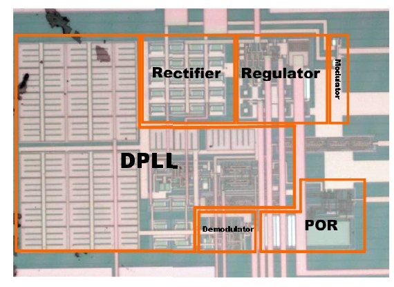
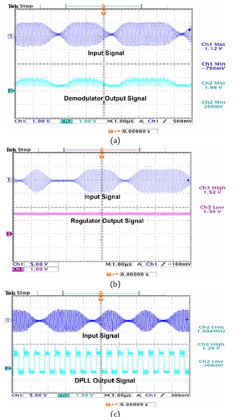
The proposed RFID AFE was fabricated using the 0.18 ㎛ CMOS standard process. The layout was done using the Cadence Virtuso and verified using the Mentor Calibre programs. The area of the AFE core is 350 ㎛ × 230 ㎛. A photo of the fabricated chip is shown in Fig. 5. The chip was packaged and then measured using an AM signal generator and an oscilloscope. Fig. 6 shows the measurement results of the fabricated chip. The measured AFE demodulator waveforms are shown in Fig. 6(a). The top and bottom signals seen in Fig. 6(a) are the input 100% modulated ASK signal and the output of the demodulator, respectively. The measured AFE regulator waveforms are shown in Fig. 6(b). The top and bottom signals in Fig. 6(b) are the input 100% modulated ASK signal and the output of the regulator, respectively. Resistors were used in the OTA feedback network. The output load capacitor for the regulator was 5 nF. From Fig. 6(b), the
output voltage of the regulator is 1.5 V, as predicted by the circuit simulations. The measured DPLL waveforms are shown in Fig. 6(c). The top signal in Fig. 6(c) is the input 100% modulated modulated ASK signal. The bottom signal is the output of the DPLL, which shows the recovered clock with the pause period of the 100% modulated ASK signal. The measurement results of the fabricated chip confirm that all the circuit blocks of our proposed RFID AFE performed as predicted by the circuit simulations.
A 13.56 MHz RFID AFE circuit for the ISO 14443 type A standard is proposed. A DPLL to recover the clock during the pause period of a 100% modulated ASK signal and LDMOSTs, made using a low voltage standard CMOS process in order to protect the rectifier and clock recovery circuit from high voltages, are used. The proposed RFID AFE circuit, using the dynamically enabled DPLL was verified by circuit simulations and fabricated using the 0.18 μm CMOS standard process. The measurement results show that the proposed RFID AFE recovers the clock for the pause period of a 100% modulated ASK signal.