Organic light-emitting diodes (OLEDs) have attracted increasing attention in recent years [1]-[5]. Today, OLEDs are considered to be one of the next generation flat- panel displays due to their low-voltage operation, wide-viewing angle, high contrast and mechanical flexibility [6]. Multilayered OLEDs (which consist of several layers such as a hole transporting layer (HTL), an electron transporting layer (ETL), an emitting layer (EML), etc.) have been studied extensively [7]. The ultimate goals are high efficiency and a long lifetime. So, many researchers have investigated the synthesis of organic materials, the optimization of structures, color tuning, etc.
White Organic light-emitting diodes (WOLEDs) have also drawn increasing attention as solid-state light sources and backlights in liquid-crystal displays and full-color OLEDs [8]-[12]. A white emission can be achieved by using two complementary colors (e.g. sky blue-red), or three primary colors (red, green, and blue). The white emission of OLEDs has a broader emission spectrum than that of inorganic emitters and the white emission of OLEDs of two complementary colors demonstrate a higher efficiency, a simpler process, and a lower shift of the exciton recombination zone than those using three primary colors. It has been reported that OLEDs are usually fabricated using an all fluorescent, an all phosphorescent, or a fluorescentphosphorescent hybrid system in EML [13]-[15]. All these phosphorescent systems have demonstrated high efficiency, but no blue phosphorescent emitters have yet been considered as a proper candidate for WOLEDs due to their short lifetime and low efficiency. All the fluorescent systems have reported stable Commission Internationale d’Eclairage (CIEx,y) coordinates and long lifetimes, but have a lower efficiency compared to all the phosphorescent and hybrid systems. Y. Sun
Indium tin oxide (ITO) coated glass with a thickness of 1000 Å supplied by LG Philips LCD was cleaned in an ultrasonic bath by the regular sequence: in acetone, methanol, diluted water and isopropyl alcohol. The precleaned ITO was then treated with an O2 plasma treatment whose conditions were 2 × 10⁻² Torr, 125 W, and 2 min. The WOLEDs were fabricated using the high vacuum (5 × 10⁻⁷ Torr) thermal evaporation of organic materials method onto the surface of the ITO (30 Ω/sq, with an emitting area of 3 mm × 3 mm) coated glass substrate. All the organic materials, except the emitters, were purified by temperaturegradient sublimation in a vacuum. The doping rates were approximately 1.0 - 1.1 Å/sec on the organic materials and 0.1 Å/sec on the lithium quinolate (Liq). After the deposition of the organic layers and without a vacuum break, the aluminum (Al) cathode was deposited at a rate of 10 Å/sec. With the DC voltage bias, the optical and electrical properties of WOLEDs such as the current density,
luminance, current efficiency, and CIEx,y coordinates characteristics were measured with a Chroma Meter CS- 100A (Konica Minolta Holdings. Inc., Tokyo, Japan) and a Keithley 236 (Keithley Instruments, Inc., Cleveland, Ohio, USA), respectively. The electroluminescence (EL) spectra of the emission from the devices were measured by a Roper Scientific Spectra Pro 300i. (Roper Scientific/Acton Research, Acton, Massachusetts, USA) All the measurements were carried out under ambient conditions at room temperature.
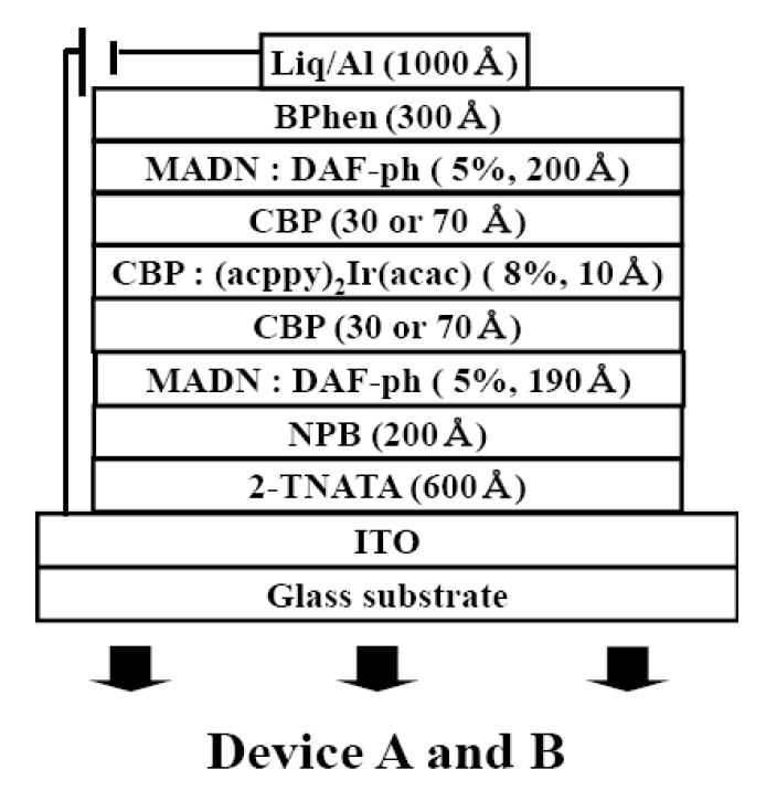
Figure 1 illustrates the device structures used in the experiment as follows: ITO as the anode (1000 A)/4,4′,4′′- tris[2-naphthyl (phenyl)amino] triphenylamine (2-TNATA) as the hole injection layer (600 A)/N,N′-bis-(1-naphyl)- N,N′-diphenyl-1,1′-biphenyl-4,4′-diamine (NPB) as the hole transporting layer (HTL) (200 A)/1,4-bis[2-(7-Ndiphenyamino- 2-(9,9-diethyl-9H-fluoren-2-yl))vinyl]benzene (DAF-ph) doped in 2-methyl-9,10-di(2-naphthyl)anthracene (MADN) as the blue EML (5%, 190 A)/CS (device A: 30 A or device B: 70 A)/iridium(III) bis(5-acetyl-2- phenylpyridinato-N,C2') acetylacetonate ((acppy)2Ir(acac)) doped CBP as the red EML (10 A)/CS (device A: 30 A or device B: 70 A)/DAF-ph doped in MADN as blue EML (200 A)/4,7-diphenyl-1,10-phenanthroline (BPhen) as the hole blocking layer and ETL (300 A)/Liq as the electron injection
layer (20 Å)/Al as the cathode (1000 Å). The doping concentration of the emitters was optimized. The emitters concentrations of DAF-ph in MADN and (acppy)2Ir(acac) in CBP were 5 and 8%, respectively.
3.2 The current density-luminance-current and the power efficiency characteristics
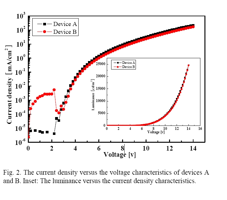
Figure 2 shows the characteristics of the current density versus the applied voltages as a function of the CS thickness. They showed a maximum current density of 212 and 168 mA/cm2 at 14 V and showed 1.11 and 1.23 mA/cm2 (nearby 1 mA/cm2) at 5.8, and 6.2 V. Device A showed a higher current density at all the voltages, which seemed to be due to carrier tunneling through the CS at the higher voltages. On the other hand, the CS of device B, with a thickness of 70 Å, does not allow the charge carriers to tunnel through the CS. As shown in the inset of Fig. 2, devices A and B had a maximum luminance of 24 600 and 24 500 cd/m2 at 14 V and the turn-on voltage of a luminance of 1 cd/m2 was about 3.6 and 3.8 V in device A and B, respectively.
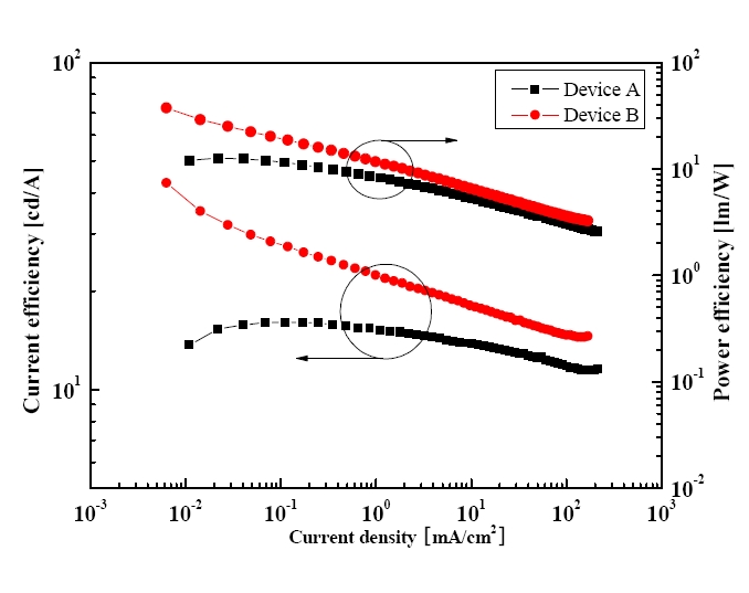
Figure 3 shows the characteristics of the current and power efficiency versus the current density. Devices A and B showed maximum current efficiencies of 16.1 and 42.9 cd/A at 0.11 and 0.006 mA/cm2 and current efficiencies of 15.2 and 22.4 cd/A at 1 mA/cm2. The devices also showed a maximum power efficiency of 12.7 and 37.5 l m/W at 0.02 and 0.006 mA/cm2 and power efficiencies of 8.25 and 11.7 l m/W at 1 mA/cm2, respectively. Device B showed a higher efficiency than device A because the CS, with a thickness of 70 Å in device B, ideally prevented the Dexter energy transfer from the phosphor triplet state of the (acppy)2Ir(acac) to the nonradiative triplet state of the DAFph or MADN. The triplet energy level of the (acppy)2Ir(acac) is higher than that of the DAF-ph and MAND. When the CS has a thickness of 30 Å, the Dexter energy transfer from the triplet state of the (acppy)2Ir(acac) to the lower nonradiative triplet state of the DAF-ph or MADN can occur, which reduces the emission from the (acppy)2Ir(acac), as shown in Fig. 4.
3.3 The electroluminescence characteristics
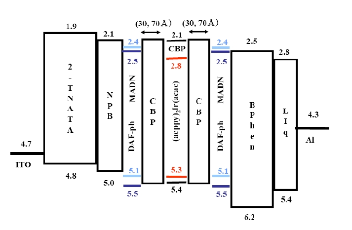
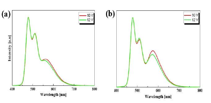
Figure 4 shows the EL spectra of devices A and B at the driving voltages of 10 and 12 V. It was also found that all the devices had two emission peaks due to the DAF-ph around 478 and 510 nm and another emission peak due to the (acppy)2Ir(acac) around 568 nm. It was shown in all three devices that the intensity of the red emission peak decreased compared to the blue and green emission peaks as the driving voltage increased. The more the thickness of the CS increased, the more the red emission increased due to the effective prevention of the triplet Dexter energy transfer from the red to the blue emitter, as shown in Fig. 5, which shows the energy level diagrams of devices A and B. The EL peaks of devices A and B can also be shown from a microcavity effect as the difference of the CS thickness.
3.4 The CIEx,y coordinates characteristics
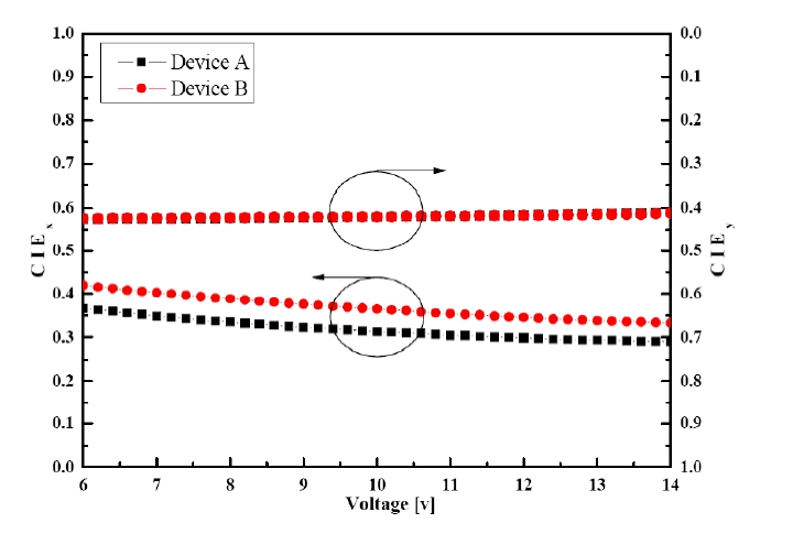
Figure 6 shows the CIEx,y coordinates changes of devices A and B as a function of the applied voltage from 6 to 14 V. All the devices showed CIEx,y coordinate changes from (0.37, 0.43) to (0.29, 0.41) in device A and from (0.42, 0.42) to (0.33, 0.41) in device B at 6 V and 14 V, respectively. It was found that the CIEx of devices A and B decreased more drastically than the CIEy of the devices as the applied
voltage increased. Device B showed a more reddish white emission at the operating voltages, which is due to the effective prevention of the triplet Dexter energy transfer as explained in Fig. 4.
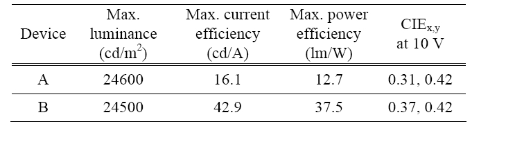
[Table 1.] The various characteristics of WOLED devices A and B.

The various characteristics of WOLED devices A and B.
Table 1 shows the various characteristics of the white devices, such as the maximum luminance, the maximum current efficiency, the maximum power efficiency, and the CIEx,y coordinates at 10 V.
It was demonstrated in this paper that highly efficient WOLEDs using blue fluorescent and red phosphorescent emitters separated by a spacer with various thickness were fabricated. The device with a CS thickness of 70 Å exhibited a maximum luminance of 24500 cd/m2, a maximum current efficiency of 42.9 cd/A, a power efficiency of 37.5 lm/W, and CIEx,y coordinates of (0.37, 0.42). The optimized device showed a current efficiency 2.5 times higher than that of the control device that had a CS thickness of 30 Å.

![The structure of devices A and B used in the experiment. Al: aluminum, Liq: lithium quinolate, , BPhen: 4,7-diphenyl-1,10- phenanthroline, MADN: 2-methyl-9,10- di(2-naphthyl)anthracene, DAFph: 1,4-bis[2-(7-N-diphenyamino-2-(9,9-diethyl-9H- fluoren-2-yl))vinyl] benzene, CBP: 4,4′-N,N′-dicarbazole-biphenyl, NPB: N,N′-bis- (1- naphyl)-N,N′-diphenyl-1,1′-biphenyl-4,4′-diamine, 2-TNATA: 4,4′,4′′- tris[2- naphthyl (phenyl)amino] triphenylamine, ITO: indium tin oxide.](http://oak.go.kr/repository/journal/10131/E1TEAO_2009_v10n6_208_f001.jpg)

![The energy level diagrams of devices A and B. The numbers showthe HOMO and LUMO of the various materials used in this study. Al:aluminum, Liq: lithium quinolate, , BPhen: 4,7-diphenyl-1,10-phenanthroline, MADN: 2-methyl-9,10-di(2-naphthyl)anthracene, DAFph:1,4-bis[2-(7-N-diphenyamino-2-(9,9-diethyl-9H-fluoren-2-yl))vinyl]benzene, CBP: 4,4′-N,N′-dicarbazole-biphenyl, NPB: N,N′-bis-(1-naphyl)-N,N′-diphenyl-1,1′-biphenyl-4,4′-diamine, 2-TNATA: 4,4′,4′′-tris[2-naphthyl (phenyl)amino] triphenylamine, ITO: indium tin oxide.](http://oak.go.kr/repository/journal/10131/E1TEAO_2009_v10n6_208_f005.jpg)