The effects of the growth temperature on the properties of ZnO thin films were investigated by using X-ray diffraction, scanning electron microscopy, ultraviolet-visible spectrophotometry, and Hall measurements. The ZnO films were deposited by rf magnetron sputtering at various growth temperatures in the range of 100-400oC. A strong c-axis preferred orientation is observed for all of the samples. As the growth temperature increases, the crystalline orientation of the ZnO (002) plane is not changed, but the full width at half maximum gets smaller. The dependence of the electron concentration, mobility, and resistivity on the growth temperature exhibits that the ZnO films have a higher electron concentration at higher temperatures, thus giving them a low resistivity. The optical transmittance and band gap energy, calculated from the spectra of optical absorbance, show a significant dependence on the growth temperature. As for the sample grown at 100°C, the average transmittance is about 90% in the visible wavelength range and the band gap is estimated to be 3.13 eV.
Over the last few decades, zinc oxide (ZnO) has been extensively investigated for its use in various industries and technologies, such as spintronics applications, light emitting diode, laser diodes, surface acoustic wave devices and transparent electrodes for solar cells and displays [1]-[3]. As for the development of ZnO-based optoelectronic devices, it is necessary to grow high-quality ZnO thin films with both n-type and p-type electrical conductions. Up to now, several methods have been used to fabricate high- quality ZnO thin films: pulsed laser deposition [4], molecular beam epitaxy [5], metalorganic chemical vapor deposition [6], direct current and radio-frequency (rf) magnetron sputtering [7], sol-gel [8], and spray pyrolysis [9]. In particular, during the growth of the films, the optimization of the growth temperature, as a method of improving their electrical and optical properties, may provide a way to control the growth rate, remove the defects and internal stress, and activate the dopants incorporated in the films.
The growth temperature is a key parameter to improve the film quality and the device performance. The use of the optimum temperature has significant effects on the dopants, defects, and stress in the ZnO films, thus changing their carrier concentration, crystalline structure, optical transmittance, and band gap energy. The growth temperature has been reported to contribute to the fabrication of highquality films, the variation of stress, the shape of the crystalline grain, the lifetime of the charge carriers, and the conduction type of the materials [10]-[13]. Ondo-Ndong
In this paper, we report the effect of the growth temperature on the structural, optical and electrical properties of ZnO thin films grown on glass substrates by rf magnetron sputtering. The properties of the ZnO films deposited at different growth temperatures are systemically investigated by X-ray diffraction (XRD), scanning electron microscopy (SEM), ultraviolet-visible (UV-VIS) spectrophotometry and Hall measurements. Furthermore, we examine how the shape of the crystalline grain, optical transmittance, band gap energy, and electrical resistivity of the ZnO thin films can be controlled by adjusting the growth temperature.
The ZnO films were grown by rf magnetron sputtering on glass (Corning 7059; USA) substrates at growth temperatures of 100, 200, 300, and 400℃. The substrates were cleaned with acetone and methanol and dried before loading in the sputtering chamber. A 2 inch-diameter ZnO target was synthesized by the conventional solid-state reaction using ZnO powders with a purity of 99.999%. The chamber was evacuated with a turbo-molecular pump to a base pressure of 5×10?6 Torr. Argon gas was used for sputtering. The working pressure was maintained at 30 mTorr at an argon flow rate of 56 sccm. The distance between the target and substrate was fixed at 50 mm. The target was presputtered for 30 min to clean its surface and attain the optimum conditions. The ZnO films were deposited at an rf power of 60 W, while rotating the substrate holder at a rate of 15 rpm.
The surface morphology of the ZnO films was characterized by field emission SEM. The crystallographic structure was investigated by XRD using Cu-Kα radiation with a wavelength of 0.154 nm. The optical absorbance was measured in the wavelength range of 300-1100 nm by means of a UV-VIS spectrophotometer. The electrical properties were examined by the van der Pauw method using a Halleffect measurement system.
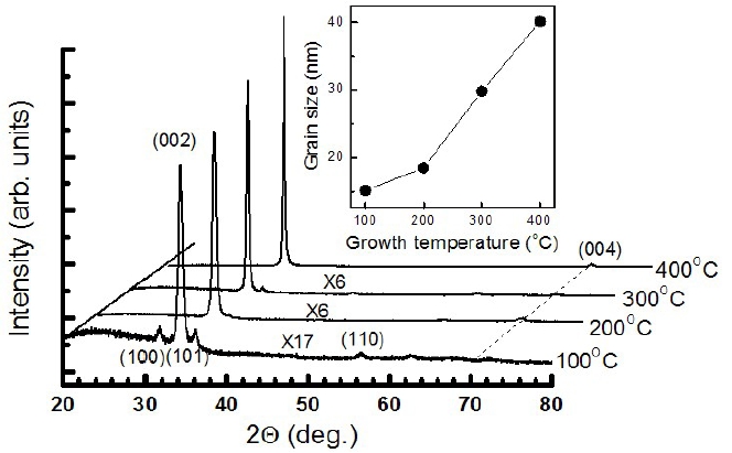
Figure 1 shows the XRD patterns of the ZnO thin films deposited on glass substrates at various growth temperatures of 100, 200, 300, and 400℃. For the sample grown at 100℃, four diffraction peaks are observed: one main peak occurs at 34.4o and three small peaks appear at 31.8o, 36.2o, and 56.6o, respectively. The former is attributed to the diffraction from the ZnO (002) plane while the latter correspond to the diffractions from the ZnO (100), (101), and (110) planes, respectively [14]. The XRD spectra of all four samples exhibit a strong (002) peak, which indicates that they have a preferential growth orientation along the c-axis perpendicular to the substrate surface. As the growth temperature is increased, the relative intensity of the (002) diffraction peak increases rapidly and its full width at half maximum (FWHM) decreases gradually, while the intensities of both the (100) and (101) peaks become smaller, so that finally, they cannot be distinguished from the background signal for the ZnO thin films grown at temperatures above 200℃. As for the ZnO film grown at 400℃, the intensity of the (002) diffraction peak is the highest and its FWHM is found to be 0.23o. These results show that the crystallinity of the ZnO thin films is enhanced as the growth temperature is increased. The well-known Scherrer crystallite size was calculated to be 15, 18, 30, and 40 nm for the films grown at 100, 200, 300, and 400℃, respectively, as shown in the inset of Fig. 1.
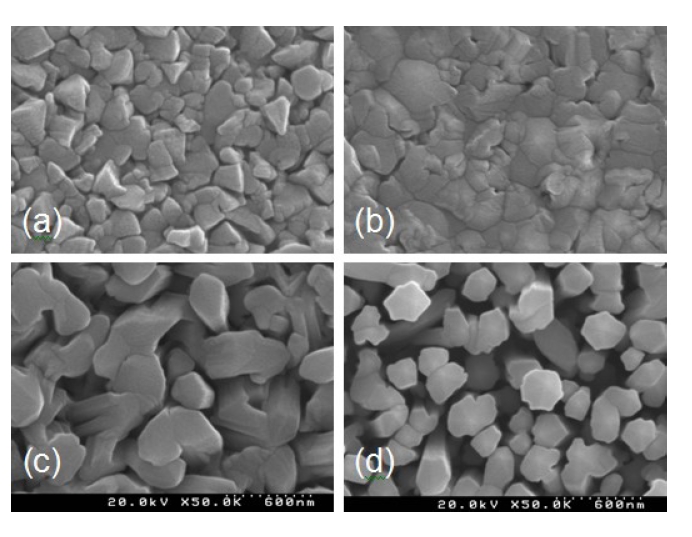
Figure 2 shows the SEM surface morphologies of the ZnO thin films grown at the four different temperatures. The lessdensely packed hexagonal-shaped crystallites developed on top of the glass substrate for the ZnO film grown at 400℃, as shown in Fig. 2(d). The crystalline grains show uniform shapes with a size of around 48 nm and a height of 300 nm, along with some pores over the films. Growing the films at a lower temperature results in the change in the shape of the crystallites and an increase in the average grain size with a closely-packed structure, as shown in Fig. 2(a) and (b). These results support the XRD measurements shown in Fig. 1, indicating that the intensity of the (002) peak is the lowest and its FWHM is the widest for the sample grown at 100℃, thus showing the deterioration of the crystallinity of the ZnO films. The crystalline grains for the film grown at 100℃ seem to be truncated trapezoids with rectangular bases. This is relatively consistent with the fact that the grain shape depends on the radio-frequency power conditions, changing from round type grains at 200 W to plate type ones at 250 W [15].
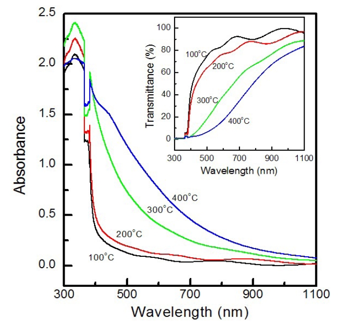
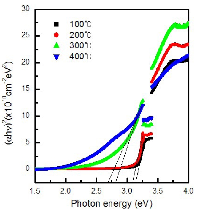
Figure 3 shows the absorbance spectra for the ZnO thin films grown at various growth temperatures. The absorption edges for the ZnO films grown at 100 and 200℃ occur at 406 and 417 nm, respectively. It can be seen that the absorption edge moves towards a higher-wavelength with increasing growth temperature. For the samples grown at 300 and 400℃, the slope of the absorbance spectra decreases slowly with a sharp sink being observed in the wavelength range of 363-379 nm, where the energy gap falls suddenly. By using the expression, A=?log[T(%) /100] , indicating the relation between the absorbance A and the transmittance T (%), we can obtain the transmittance as
The inset of Fig. 3 shows the wavelength dependence of the optical transmittance spectra for the ZnO thin films grown at the four different growth temperatures obtained using Eq. (1). As for ZnO films grown at 100 and 200℃, an oscillation phenomenon of the transmittance spectra and an average transmittance of about 90% are observed in the wavelength range from 600 to 1100 nm. It is well known that this oscillation results from the light interference at the interface between the ZnO film and the glass substrate [16].
The optical band gap of the ZnO films can be calculated from the relationship between the optical absorption coefficient and the transmittance. The absorption coefficient α near the absorption edge is given by α = ? ln
where A is a proportional constant,
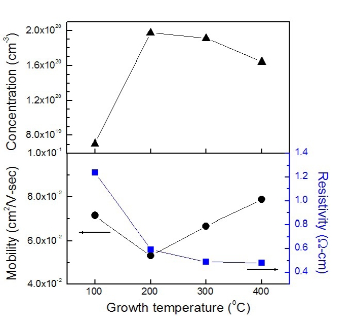
Figure 5 shows the electron concentration, mobility, and electrical resistivity of the ZnO thin films as a function of the growth temperature. The ZnO film grown at 100℃ was found to have an electron concentration of 7.1×1019 cm-3, a Hall mobility of 0.07 cm2V-1s-1, and an electrical resistivity of 1.2 Ωcm. As the growth temperature is increased, the electron concentration approaches the maximum value for the sample grown at 200℃ and then decreases gradually, while the electrical resistivity decreases rapidly in the growth temperature range of 100-200℃ and remains almost constant at 300 and 400℃. On the other hand, the mobility
shows a minimum value for the sample grown at 200℃. The decrease in the mobility at a growth temperature of 200℃ is mainly due to the increase in the carrier concentration, rather than the decrease in the electrical resistivity. These results support the expression that the electrical resistivity ρ is inversely proportional to the electron density n and mobility μ , as described by the well-known equation, ρ = 1/μ
The effect of the growth temperature on the structural, optical and electrical properties of ZnO thin films was investigated by X-ray diffraction, SEM, UV-VIS spectrophotometry and Hall measurements. The intensity of the ZnO (002) peak for the film grown at 400℃ is the highest and its FWHM is measured to be 0.23°. With increasing growth temperature, the optical band gap and electrical resistivity decrease significantly and an improvement of the ZnO film’s crystallinity is observed. The optical transmittance for the ZnO film grown at 100℃, obtained from its optical absorbance spectrum measured at room temperature, is found to be 92% at 700 nm.