Transparent and conducting ITO/Cu/ITO multilayered films were deposited by magnetron sputtering on unheated polycarbonate (PC) substrates. The thickness of the Cu intermediate film was varied from 5 to 20 nm. Changes in the microstructure and optoelectrical properties of ITO/Cu/ITO films were investigated with respect to the thickness of the Cu intermediated layer. The optoelectrical properties of the films were significantly influenced by the thickness of the Cu interlayer. The sandwich structure of ITO 50 nm/Cu 5 nm/ITO 45 nm films had a sheet resistance of 36 Ω/Sq. and an optical transmittance of 67% (contain substrate) at a wavelength of 550 nm, while the ITO 50 nm/Cu 20 nm/ITO 30 nm films had a sheet resistance of 70 Ω/Sq. and an optical transmittance of 36%. The electrical and optical properties of ITO/Cu/ITO films were determined mainly by the Cu film properties. From the figure of merit, it is concluded that the ITO/Cu/ITO films with a 5 nm Cu interlayer showed the better performance in transparent conducting electrode applications than the conventional ITO films.
The Sn doped indium tin oxide (ITO) thin films are highly degenerate, wide-gap semiconductors with good conductivity and high optical transmission across the visible spectrum [1]-[4]. Recently, there has been considerable interest in the use of ITO films deposited on polymer substrates for application as flexible display devices due to the fact that they more lightweight and flexible than ITO films prepared on glass substrates. However, it is difficult to deposit high quality ITO thin films on polymer substrates as there is a restriction on the substrate temperature during the deposition process.
One way to improve the optical and electrical properties of ITO films deposited on polymer substrates is to use ITO/metal/ITO (IMI) multilayer films, which have lower resistivity than ITO single-layer films of the same thickness [5], [6]. In recent years, Ag metal films, which have the highest conductivity of all metals, have been used for ITObased multilayers for low resistance and transparent electrodes [7]. However, there are few reports related to Cu and ITO based multilayers for application in low resistance transparent electrodes.
In this study, ITO single-layer and ITO/Cu/ITO multilayer films were deposited on polycarbonate (PC) substrates by RF and DC magnetron sputtering. The thickness of the Cu interlayer was varied from 5 to 20 nm. Changes in the microstructure and opto- electrical properties of the ITO/Cu/ITO films with various thicknesses of Cu interlayer were investigated using X-ray diffraction (XRD), Hall Effect measurements, and UV- Visible spectrometry, respectively.
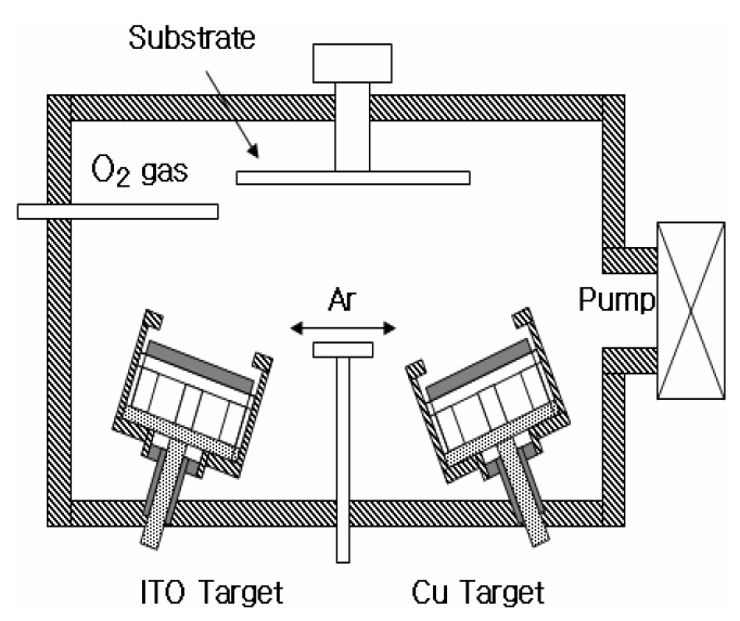
Thin films of ITO and ITO/Cu/ITO were deposited on PC substrates using an ITO (99.99 purity, 7.62 cm diameter, 0.5 cm thickness) and metal Cu target (99.9 purity, 7.62 cm diameter) in a magnetron sputter plant equipped with two cathodes. RF (13.56 MHz) and DC power were applied to ITO (purity; 99.99%) and Cu (purity; 99.99%) targets, respectively. The target was a 4-in diameter, 0.25-in thick, sintered In2O3 (90%) + SnO2 (10%) pure Cu disk. ITO/Cu/ITO layered films were deposited on an unheated PC substrate (10×10 cm2 size, 100 μm thick). Although the PC substrate was not heated intentionally, the substrate temperature increased to 70℃ during deposition. The substrate temperature was monitored using a k-type thermocouple directly in contact with the substrate surface. Figure 1 shows the experimental magnetron sputtering system.
Prior to deposition, the chamber was evacuated to 1.3×10⁻⁴ Pa. The ITO films were deposited in an argon (Ar) and oxygen (O2) gas mixture adjusted for minimum resistivity
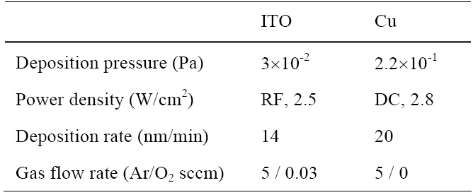
[Table 1.] Deposition conditions of ITO and Cu thin films.

Deposition conditions of ITO and Cu thin films.
[Table 2.] Composition of ITO/Cu/ITO multilayer films.
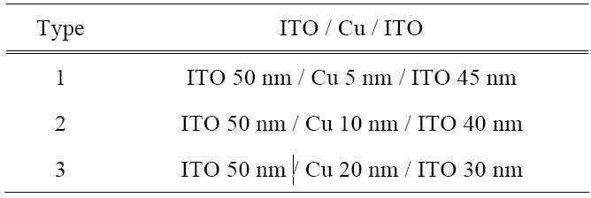
Composition of ITO/Cu/ITO multilayer films.
films at 3×10⁻¹ Pa. The intermediate Cu films were deposited in a pure Ar atmosphere at 1×10⁻¹ Pa. A deposition distance of 10 cm between the target and substrate was maintained and the substrate rotation speed was set to 10 rpm for all depositions. By controlling the deposition time, a thickness of 100 nm was achieved in both ITO and ITO/Cu/ITO films. In ITO/Cu/ITO films, the thickness of the intermediate Cu film was 5, 10 or 20 nm. Table 1 and 2 show the experimental deposition conditions and composition of the ITO/Cu/ITO films, respectively.
The film thickness and presence of Cu in IMI films were confirmed with a surface profilometer and secondary ion mass spectroscopy (SIMS, IMS 6f, CAMECA) at the Korea Basic Science Institute (KBSI). The optical absorption and transmittance were measured between wavelengths of 300 and 900 nm for all IMI films and uncoated PC substrates by a UV-Vis. spectrophotometer referenced with air. The transmission of the multilayers, including the PC substrate, is presented in this paper. The optical transmittance of the uncoated PC substrate is also shown for comparison. XRD was used to observe the thin film crystallinity of ITO and IMI films. In addition, prior to intermediate Cu deposition, 50 nm thick ITO films in the IMI structure were also measured by XRD. Electrical properties of the films were evaluated by Hall Effect measurements. After deposition, the performance of the ITO/Cu/ITO films as transparent conducting films was evaluated using a figure of merit.
In a conventional magnetron sputtering process, a high substrate temperature or annealing temperature of 200 - 300℃ is required to provide polycrystalline ITO films. Sun et al. [8] investigated the initial growth mode of ITO on a glass substrate within a substrate temperature range of 20 - 400℃ and suggested that ITO films with an amorphous structure formed at substrate temperatures below 150℃.
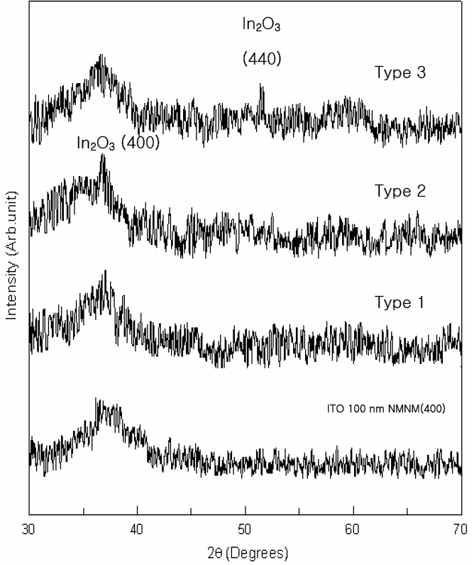
Figure 2 shows the XRD pattern of ITO and ITO/Cu/ITO films.
None of the ITO and ITO/Cu/ITO films showed any strong diffraction peaks in the XRD pattern. This was due to the low substrata temperature and too thin films to form crystalline phase. It is supposed that the Cu interlayer in ITO/Cu/ITO films is not effective in the crystallization of the ITO films at low substrate temperatures.
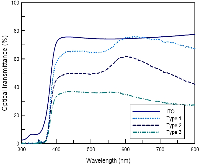
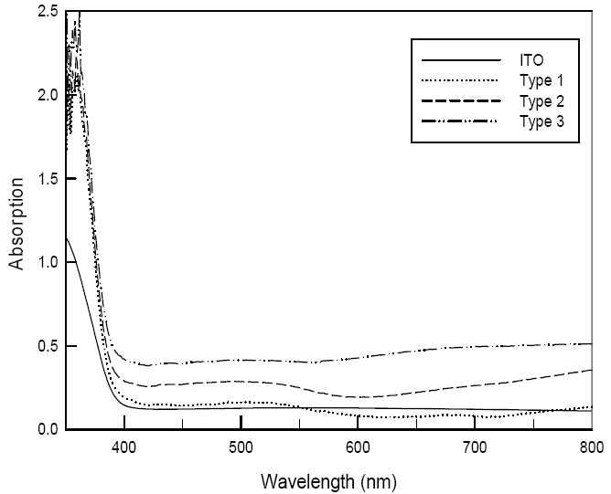
Figures 3 and 4 show optical transmittance and absorption respectively for a wavelength range of 300 - 800 nm.
In Fig. 2, a bare PC substrate and ITO film had 90% and 74% (contains PC substrate) transmittance respectively at 550 nm, relative to the transmittance air. This is consistent with previously reported conventional magnetron sputtering results without substrate heating [9]. ITO films with 5 nm Cu interlayer showed the highest observed optical transmittance of 67% at 550 nm. The transmittance decreased with increasing Cu interlayer thickness. ITO films showed lower optical absorption and as the Cu thickness increased the absorbance of the films increased, as shown in Fig. 4.
Along with optical analysis, the electrical properties of the films were evaluated with Hall Effect measurements. Table 3 shows the electrical properties of ITO and ITO/Cu/ITO films such as carrier density, carrier mobility and electrical resistivity. As the thickness of the Cu interlayer increased, the carrier concentration increased initially from 2.7× 10²⁰/cm3 (Type 1) to 5.4×10²¹/cm3 (Type 2) and decreased to 1.2×10²⁰/cm3 for the Type 3 film.
In this study, Cu interlayer was prepared with different thicknesses ranging from 5 to 20 nm in ITO/Cu/ITO films. Since Cu films have a high diffusion coefficient, the metal can diffuse into the ITO films. The diffused Cu substitutes the indium site of the ITO films and Cu produces Cu2+ ions, while the indium produces In3+. Because of the difference in valances of Cu2+ and In3+, the Cu substitutions may reduce
electrons in the ITO matrix [10]. Thus the decrement in carrier density (1.2×10²⁰/cm3) in ITO 50 nm/Cu 20 nm/ITO 30 nm films was attributed to Cu substitution at the In site of the ITO films.
The electrical resistivity, which was influenced by carrier concentration, also decreased from 3.6×10⁻⁴ Ωcm (Type 1) to 1.5×10⁻⁴ Ωcm (Type 2). However, the electrical resistivity of Type 3 increased to 7×10⁻⁴ Ωcm due to reduced carrier density.
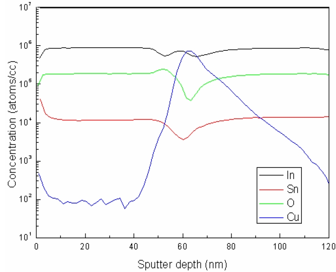
Figure 5 shows the SIMS depth profile obtained from the ITO 50 nm/Cu 5 nm/ITO 45 nm films. The Cu ion intensity in the middle indicates the presence of a Cu interlayer in the IMI films.
The figure of merit (FTC) is an important index for evaluating the performance of transparent conducting oxide films. The FTC is defined as
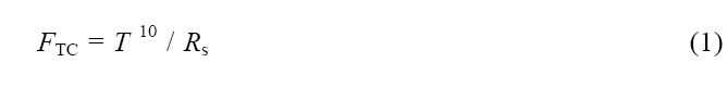
where T is the optical transmittance (at 550 nm) and Rs is the sheet resistance [11]. In Table 3, the FTC reached a maximum of 5.2×10⁻⁴ Ω-1 for ITO 50 nm/Cu 5 nm/ITO 40 nm multilayer films. This value was greater than the FTC of ITO single layer films (1.6×10⁻⁴ Ω-1) and other compositions considered in this study. Type 3 in Fig. 3 had a thicker Cu layer in the interlayer and did not exhibit sufficient optical
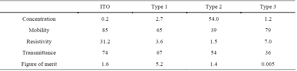
Comparison of carrier density (×1020/cm3), carrier mobility (cm2/Vs), electrical resistivity (×10-4 Ω cm), optical transmittance at 550 nm and figure of merit (×10-4 Ω-1, φ TC) of ITO single and ITO/Cu/ITO multilayer films.
transmittance to be used as a transparent conducting electrode. A greater FTC results in better transparent conducting oxide (TCO) films. Thus the ITO/Cu/ITO films with a 5 nm Cu interlayer showed a better performance than ITO films in transparent conducting electrode applications.
ITO single and ITO/Cu/ITO multilayered films were deposited without intentional substrate heating on PC substrates using a magnetron sputtering processes. The influence of the thickness of Cu interlayer in ITO/Cu /ITO films on opto-electrical properties was investigated. A high quality, transparent ITO film with a 5 nm Cu intermediate film in an IMI electrode with a resistivity as low as 3.6×10⁻⁴ Ω cm and a high optical transmittance of 67% at 550 nm with respect to air was obtained. Based on the figure of merit, it is clear that ITO/Cu/ITO multilayer films with a 5 nm Cu intermediate film have a better performance in transparent conducting electrode applications than have ITO single-layer films.