For integrated passive device (IPD) applications, we have successfully developed and characterized metalinsulator- metal (MIM) capacitors with 2000 A plasma-enhanced chemical vapor deposition (PECVD) silicon nitride which are deposited with the SiH4/NH3 gas mixing rate, working pressure, and RF power of PECVD at 250℃. Five PECVD process parameters are designed to lower the refractive index and lower the deposition rate of Si3N4 films for the high breakdown electric field. For the PECVD process condition of gas mixing rate (0.957), working pressure (0.9 Torr), and RF power (60 W), the atomic force microscopy (AFM) root mean square (RMS) value of about 2000 A Si3N4 on the bottom metal is lowest at 0.862 nm and the breakdown electric field is highest at about 8.0 MV/cm with a capacitance density of 326.5 pF/mm2. A pretreatment of metal electrodes is proposed, which can reduce the peeling of nitride in the harsh test environment of heat, pressure, and humidity.
The continuing trend towards greater miniaturization of electronic systems has increased the demand for highperformance, high-integration, high-yield, and low-cost products. Owing to the fact that IPDs are generally fabricated using standard fabrication technologies such as thin film and photo-lithography processing, they can be manufactured with the above-mentioned advantages and widely used in the front-end RF sections [1].
Silicon nitride is widely used in the manufacturing processes of various compound semiconductor devices and circuits. These processes include device passivation of metal semiconductor field-effect transistors (MESFETs) [2], high electron mobility transistors (HEMTs) [3], [4], heterojunction bipolar transistors (HBTs) [5]-[7], sensitive layer for pH-ISFET [8], [9], dielectric layers for MIM capacitors [10] and wafer-level encapsulation to protect the circuit against environmentally induced mechanical scratches.
MIM capacitors occupy a large fraction of the die area in IPDs and other monolithic microwave integrated circuits (MMICs), so that the insulator thickness of MIM capacitors has to be reduced to increase the capacitance. However, as the dielectric thickness is reduced, the effect of bottom metal roughness and other defects becomes more dominant, and it is more difficult to maintain the breakdown electric field and the reliability of the capacitor.
One way to obtain high yield MIM capacitors is to decrease the bottom metal roughness. This is because a rough surface and the corner of the bottom metal can create poor coverage within the Si3N4 dielectric deposition, which could cause a serious capacitor electrical short [11]. In order to improve the smoothness of the bottom metal, we propose some methods, such as source wiping, pre-melting, Au dry- etching post-treatment, and metal evaporation rate adjustment. Chemical wiping of source pellets can also remove surface contaminants.
In this study, MIM capacitors with 2000 A thick silicon nitride layers are manufactured with the SiH4/NH3 gas mixing rate, working pressure, and RF power of the PECVD process at 250℃ chamber temperature. We obtained good MIM capacitors with very high breakdown electric fields (8.0 MV/cm) and a capacitance of about 326.5 pF/mm2, which could be applicable for mass production because of their good uniformity. In the case of a 13.06 pF MIM capacitor (200 μm × 200 μm electrode area), a 97% yield and up to 148 V breakdown voltage can be obtained. Finally, we report on the benefits of pre-deposition treatments of N2 annealing and O2/H2 plasma treatment, which can enhance nitride adhesion and improve the consistency of MIM capacitor reliability performance.
In order to improve the yield of MIM capacitors used for the IPDs, methods such as source wiping, pre-melting, dryetching post-treatment, and metal evaporation rate adjustment were proposed. In order to improve the breakdown electric field, silicon nitride is deposited at 250℃ by PECVD whose process parameters consist of the SiH4/NH3 gas mixing rate, working pressure, and RF power. The refractive index of the silicon nitride thin films can be measured by an ellipsometer, and the surface roughness can be analyzed by AFM.
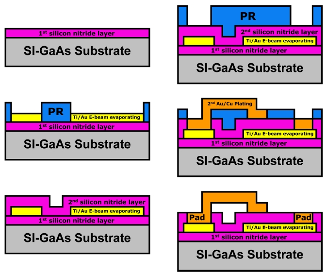
Figure 1 shows the process for fabrication of the MIM capacitors, which is used in the true IPD process. This process starts with a first passivation layer which is composed of Si3N4 and is deposited by PECVD with a thickness of 2000 A. This layer is necessary to attain an even surface over the defects and roughness of the substrate
[Table 1.] Bottom metal roughness optimization proposal and measured results.
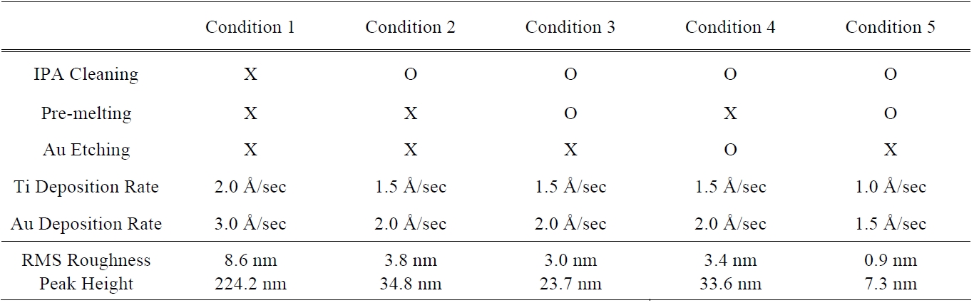
Bottom metal roughness optimization proposal and measured results.
surface. After the deposition of Si3N4, the wafer is masked by a photo resistor to define the structures of the first metal layer. Then, a 50/450 nm-thick Ti/Au metal layer is formed by electron beam evaporation, which is used as the bottom metal layer of the MIM capacitor. At this moment, the middle dielectric part of the MIM capacitor is realized. A Si3N4 of 2000 A is deposited by PECVD and masked to define the structure. After the deposition step, a reactive ion etch (RIE) in oxygen/SF6 is performed to remove the undesired layer of the Si3N4.
Next, a 1000 A-thick Ti/Au seed metal layer followed by an air-bridge post-photo process is deposited by sputter. Then, an air-bridge photo process is performed prior to both the Cu/Au (6.5 μm/0.5 μm) second metal definition and plating process. The Cu/Au plating is performed to make the top electrode pad and the air bridge for an MIM capacitor. Thus an MIM capacitor is formed with the first metal bottom plate, the second metal top plate, and a dielectric layer. After the electroplating process, the air-bridge mask is stripped, and the dry-etching step of the Ti/Au seed metal is done. Finally, all components are passivated with 3000 A Si3N4 to protect them from oxidization and moisture.
3.1 Bottom metal surface roughness of MIM capacitor
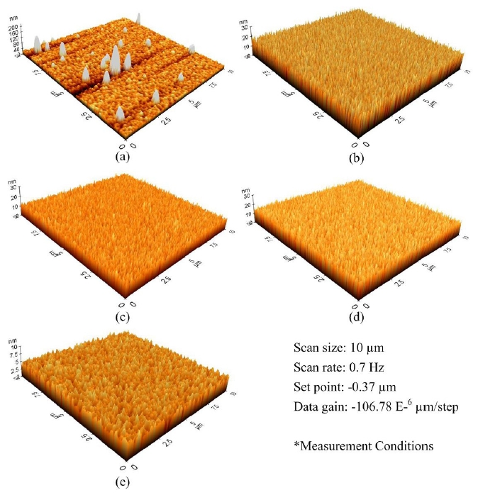
By cleaning the metal source in an ultrasonic methanol bath and implementing isopropyl alcohol (IPA) pretreatments, the bottom metal surface becomes much smoother. When this cleaning is implemented in conjunction with wiping the carbon residue off the gold melt prior to each run, the defective level is reduced by five times and yields are improved [12]. Pre-melted materials offer a more constant composition and surface topography compared with the irregular surface of a pile of randomly sized pieces. So the evaporation proceeds more smoothly. Au dry-etching post-treatment and metal evaporation rate adjustment are also considered. All the conceivable conditions are displayed in Table 1. Figure 2 shows five cases of surface roughness, all of which are measured by AFM. After IPA cleaning, the
[Table 2.] PECVD process conditions and properties of the Si3N4 films.
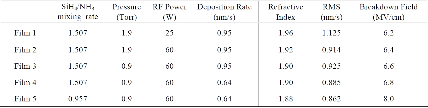
PECVD process conditions and properties of the Si3N4 films.
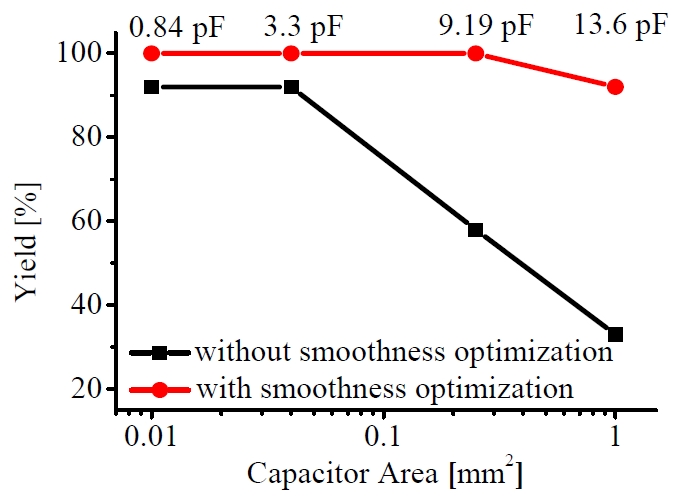
metal surface roughness can be greatly reduced. The surface roughness achieved with condition 4 is slightly less than that obtained with condition 2. However, we note that Ar-plasma Au dry-etching treatment increases the sheet resistance value of thin film resistor (TFR), so it cannot be recommended. Through condition 2, it is found that the effect of premelting is obvious. On the basis of IPA pre-cleaning and metal pre-melting, decreasing the metal deposition rate can reduce the surface roughness. Obviously, condition 5 with source cleaning and pre-melting under a lower evaporation rate shows the best smoothness. Through the bottom metal smoothness optimization strategy, MIM capacitor yield is improved as shown in Fig. 3.
3.2 Properties of the dielectric layer of MIM capacitor
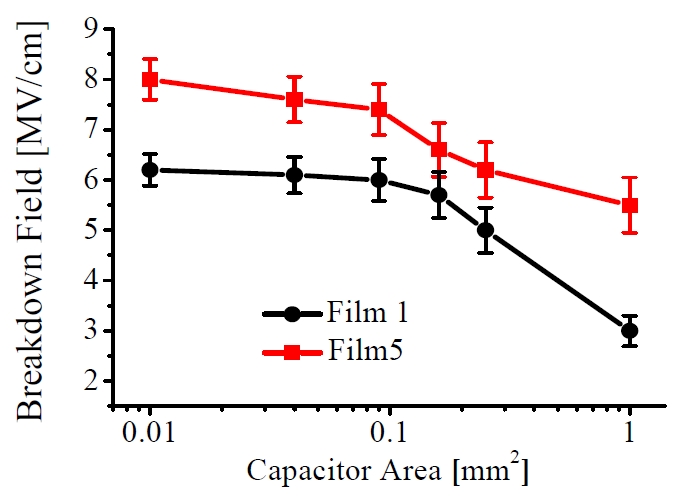
The breakdown electric field mainly depends on the insulator surface morphology and the Si-H bonding of silicon nitride thin films. In this paper, PECVD process parameters such as the SiH4/NH3 gas mixing rate, working pressure and RF power at a 250℃ chamber temperature are designed to lower the refractive index for the high breakdown electric field. Five PECVD process conditions of the insulator layers and the properties of these insulator layers are summarized in Table 2. Figure 4 shows the breakdown electric field of MIM capacitors for films 1and 5. Obviously, the breakdown electric field of film 5 is much better than that of film 1. Since the amount of Si in the film increases, while that of N decreases, the refractive index of the Si3N4 thin films increases as the SiH4/NH3 flow ratio increases. The NH3 flow deposited N atoms on to the film by bringing about the dissociative adsorption of the SiNH or SiH species. This increase in refractive index is due to the decreased N-H bonding that occurs with decreasing N content. Usually, the increase in the pressure can increase the refractive index, which is attributed to an increase in the Si content. By increasing the working pressure of PECVD, the number of ions generated in the plasma increases, which results in a larger ion flux reaching the substrates [13]-[16]. By decreasing the deposition rate, the surface roughness can be greatly reduced.
In summary, to manufacture MIM capacitors with a high breakdown electric field, a lower working pressure, a higher RF power and a lower deposition rate are needed, which can reduce the surface roughness and increase the density of Si3N4 film. Then, an increase of Si-H bonding as the NH3 gas mixing rate increases is needed, which can reduce the refractive index of Si3N4.
3.3 MIM capacitor for the true SI-GaAs IPDs
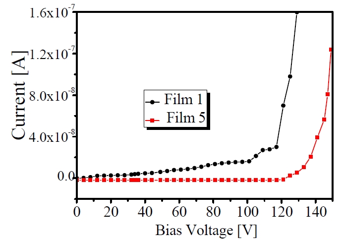
Figure 5 shows the current-voltage curves of MIM capacitors fabricated using films 1 and 5. These curves are used to interpret the breakdown electric field of MIM capacitors at 100 nA leakage current. MIM capacitors of film 5 have a higher breakdown voltage and a lower leakage current at pre-breakdown region than film 1. The breakdown
electric field of film 5 is about 8.0 MV/cm, and the breakdown voltage is about 148 V. There is a reliability problem in respect of film 1; due to the high incipient leakage current, the MIM capacitor is subjected to a continuous electrical stress which leads to a continuous leakage current that degrades MIM capacitors at the bias voltage or current. The data for all films are measured using a DC measurement system, which consists of a probe station and a parameter analyzer.
[Table 3.] Comparison of film 6 incorporating pre-deposition treatment with film 5.

Comparison of film 6 incorporating pre-deposition treatment with film 5.
3.4 Reliability test of MIM capacitor
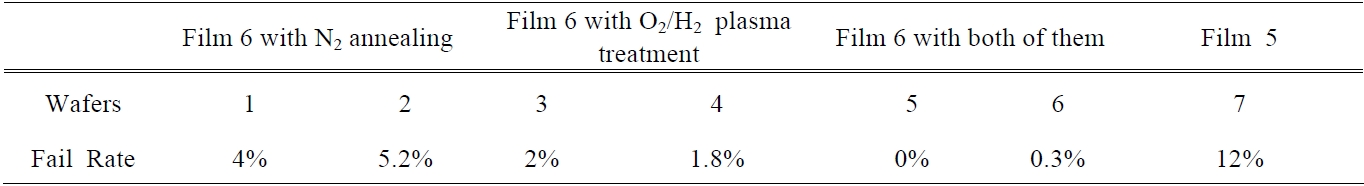
In order to test the reliability performance of nitride films, we performed a pressure cooker test (PCT) on MIM capacitors. The breakdown voltage and leakage current are tested when the I-V characteristics are measured up to 150 V. Film 5 shows a typical failure rate of 12%, however, we note that there is a severe breakdown voltage degradation from film 1 with a typical failure rate which is 5 times or greater than the worst result for film 5.
To improve the reliability of the consistency of silicon nitride film, the pre-deposition treatment is explored. Predeposition treatment, including N2 annealing and O2/H2 plasma treatment, which are evaluated on film 5 (we call it film 6) are shown to improve the consistency of the reliability performance of MIM capacitors. With the predeposition treatment, the breakdown failure rate from film 6 is almost zero, so that a notable benefit of pre-treatment highlights how an interface between the nitride and the metal electrode (Au) plays a crucial role in the reliability of the MIM capacitors. We propose a possible mechanism for removing this organic and oxidative contamination of the metal surface, which is to use N2 annealing or O2/H2 plasma treatment. These processes enhances nitride adhesion to the metal electrode and reduces the delamination of the nitride thin film in the high-pressure, high-temperature, and highhumidity environment of the PCT. The breakdown failure rate from film 6 (with the pre-deposition treatment) was compared to film 5 (without pre-deposition surface treatment) and summarized in Table 3.
In order to increase the yield of MIM capacitor, IPA precleaning, metal pre-melting, and metal evaporation rate adjustment are proposed in this study. For the PECVD process, MIM capacitors have been manufactured with a high breakdown electric field. The refractive index of silicon nitride is decreased by decreasing the SiH4/NH3 gas mixing rate and the density of silicon nitride is increased by increasing the working pressure and RF power. As the SiH4/NH3 gas-mixing rate and deposition rate are decreased, the RMS values of silicon nitride thin films are decreased and the breakdown electric fields are improved. These results imply that the breakdown electric field depends on the surface morphology and the Si-H bonding of silicon nitride thin films. Furthermore, the incipient leakage current is also increased when the working pressure and RF power are not optimized in the PECVD process.
The results observed from both films in reliability performance confirmed that the film composition, particularly the Si to N ratio, which is crucial for MIM capacitor reliability. Pre-deposition treatments, including N2 annealing and O2/H2 plasma treatment, are evaluated to show the improvement in reliability of the MIM capacitor and the reduction of performance variability.
MIM capacitors were fabricated with a high yield and high breakdown electric field as proposed. The breakdown electric field and capacitance were about 8.0 MV/cm and 320 pF/mm2 ±10%, respectively. Their property yield for mass productivity is above 97% and the breakdown voltage is over 148 V in the case of 13.06 pF MIM capacitor.