A dual mode liquid crystal display (LCD) has been introduced as a multi-functional display due to its capability to be operated in both dynamic and memory LCD modes in a display panel [1-3]. The dynamic mode has only one permissible state in the absence of an external field so that it is suitable for displaying moving images that require fast response time [4-9]. On the other hand, the memory mode has two stable states without an external field so that this is well suited to displaying texts or still images, with low power consumption [10-13].
Recently, we have proposed a transflective configuration of a dual mode LCD, which has transmissive and reflective parts in its pixels for dynamic and memory modes, respectively [3]. The transflective configuration can maximize the power efficiency of a display application by reducing the power consumption of a light source when the LCD is operated in its memory mode. However, the proposed configuration shows a poor contrast ratio of under 5:1 for the memory mode due to light leakage over the entire visible light wavelength range, except for a selected central wavelength at the dark state, as well as non-optimized parameters of the LC cell for the transmittance at the bright state.
In this paper, a transflective configuration of a dual mode operating LCD is proposed. It applies a wideband structure to the reflective part for the memory mode to enhance the contrast ratio. The wideband structure plays an important role in suppressing the light leakage in the splay state, and in realizing good dispersion properties for the entire visible range. The transmissive part for the dynamic mode can also be designed to have the same cell-gap and rubbing direction as those of the reflective part. In order to obtain high reflectance for the memory mode, as well as control the driving voltage and transmittance for the dynamic mode, the parameters of the LC cell and compensation films have been optimized. The parameters of the LC cell are optimized using the Jones matrix method, and the results are verified by the measured values of the fabricated LC cell, using the proposed configuration.
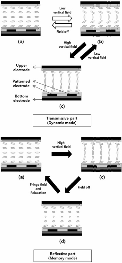
Fig. 1 shows the operating principle of our transflective dual mode LCD. The upper and lower parts represent transmissive dynamic and reflective memory modes, respectively. Our transflective dual mode LCD has the same rubbing angle and cell gap in both dynamic and memory modes. For applying vertical and fringe fields, we use upper, patterned and bottom electrodes on upper and bottom substrates. A LC mixed with a chiral dopant (thicknessto- pitch (d/p) ratio of 0.25) was inserted between two parallelly rubbed substrates. Initially the cell is in a splay state (Fig. 1(a)). Here, we will show the operating principle and LC director profiles depending on applied fields, which are drawn in Fig. 1, for the two modes. If we apply an appropriate vertical field, the splay state is transformed to a low bend state (Fig. 1(b)). If we increase the vertical voltage, the low bend state is switched to a high bend state (Fig. 1(c)). Hence, the transmissive dynamic mode is realized between these two states, as optically compensated bend (OCB) mode. In the reflective memory mode, splay (Fig. 1(a)) and π-twist states (Fig. 1(d)) are used as two stable states. In order to switch from the splay state to the π-twist state, we apply a high vertical field between the upper and bottom substrates. The LC molecules will transit into a high bend state (Fig. 1(c)). Then, if we remove the vertical field, the high bend state relaxes into a topologically equivalent π-twist state (Fig. 1(d)). We can also switch from the π-twist state to the initial splay state by applying a fringe field between the bottom and patterned electrodes.
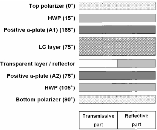
Fig. 2 shows the proposed configuration of a transflective dual operating mode LCD, which is composed of an upper compensation layer, an LC cell, a transparent layer/reflector and a lower compensation layer. The upper compensation layer plays a role in realizing a completely dark state over the entire visible light wavelength range of the memory mode, by forming a wideband structure with the LC cell. The transparent layer and the reflector divide each pixel into the transmissive and reflective parts, respectively. The lower compensation layer is able to cancel the retardation values of the upper compensation layer and the LC cell, as well as to determine the driving voltage of the dynamic mode. The detailed structure and parameters of the upper and lower compensation layers and LC cell can be optimized by performing the following design process.
In order to realize a contrast ratio over 10:1 for the memory mode, firstly, the upper compensation films and the LC layer were designed as a wideband quarter-wave structure, and their optical parameters were optimized. In previous research, it was proposed that an adequate combination of a half-wave plate (HWP) and a quarter-wave plate (QWP) can provide complete dark state over the entire visible light wavelength range for the reflective LCD, when the directions of the optic axes (OAs) of the HWP and QWP, with respect to the transmission axis (TA) of the polarizer, were determined as below [14, 15]:
where θQWP and θHWP are the angles of OAs of the QWP and HWP, respectively. By substituting the non-twist quarter-wave LC layer for the QWP, we could control the transmittance of the dark state below 10% with respect to that of the bright state in the entire visible range. The upper compensation layer is composed of a HWP and a positive A-plate (A1). The OA of A1 is oriented perpendicular to the rubbing direction of the LC layer. In order to obtain high transmittance in dynamic operation, it is advantageous that the low bend state has a larger retardation value than a half retardation at the designed wavelength. Therefore, the retardation value of the splay state for the memory mode should be more than that of the designed wavelength. By the calculation, the cell-gap margin is acceptable. However, the color shift at oblique angle and the viewing angle properties of the LC cell are not acceptable, need more improvement. A1 makes it possible to control the cell-gap, arbitrarily, by canceling the retardation value of the LC layer. As a result, the control of the cell-gap is important for achieving high transmittance and high reflectance for the dynamic and memory parts, respectively. By canceling the retardation value of the splayed LC layer, the sum of the retardation values of the A1 and the LC layer can be equalized to that of the quarter-wave plate (QWP). The retardation value of A1 must satisfy the following condition:
where RLC and RA1 are the retardation values of the LC layer of the splay texture and the A1, respectively.
In order to obtain high reflectance at the π-twist state of the memory part, under the condition of the wideband quarter-wave structure, the cell-gap and retardation values of A1 were optimized by using the Jones matrix method [16]. The reflectance, R, of the proposed configuration can be calculated as follows:

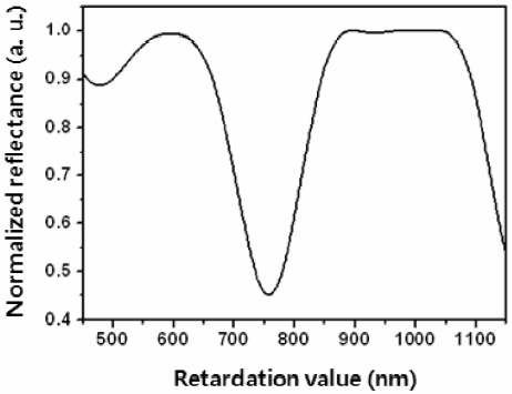
where V and V' are the incident and reflected Jones vectors, MH, MA1(RA1), MLC(RLC) are the Jones matrices of the HWP. The tilde over the MLC indicates the transposition operation. Using (3), the reflectance of the π-twist state was calculated with respect to the retardation value of the LC layer, as shown in Fig. 3. In Fig. 3, maximum transmittances exist at the retardation values of about 650 and 1003.5 nm. Because in the second maximum value the cell gap tolerance is good and enough retardation can be obtained in the bend state of dynamic mode, we chose the retardation value of the LC layer as 1,003.5 nm.
We used the one dimensional optical simulator, Dimos 2.0 for the optical design of the dynamic mode. A LC MLC-6224-000 (Merck KGaA) is used for the calculation and the elastic constants are K11=13.1 pN, K22=6.23 pN and K33=22 pN. The pretilt angle and retardation value are 4° and 1003.5 nm, respectively. During the simulation, we assumed that the LC is aligned homogeneously in splay state. The configuration of the transmissive dynamic part was designed to have the same rubbing direction and retardation value as the LC layer and the upper compensation layer of the reflective memory part. The role of the lower compensation layer cancels the retardation of the upper compensation layer and the residual retardation near the surface in the LC layer of the high bend state. The lower layer is composed of a HWP and a positive A-plate (A2). The lower HWP cancels the retardation value of the upper one. The OA of the lower HWP is oriented perpendicular to the upper one. A2 plate should be designed by considering the retardation values of A1 in the high bend state. The retardation value of A2 is given by
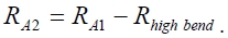
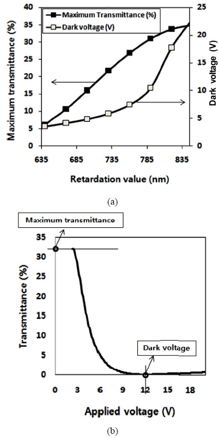
where, Rhigh bend and RA2 are the retardation values of the LC cell of the high bend state and A2. The angle of the OA of A2 is in the same direction as the rubbing direction, in order to cancel the retardation values of A1. If the entire cell satisfies the condition of (4), the cell is perfectly compensated. A2 affects the transmittance of the low bend state as well as the dark voltage of the high bend state in the dual mode LC cell. In order to obtain high brightness and low driving voltage for the dynamic mode, the retardation value of A2 was optimized. The maximum transmittance and driving voltage of the dynamic mode which were calculated and shown in Fig. 4(a) are dependent on the retardation value of A2. The maximum transmittance in Fig. 4(a) means a specific transmittance of the cell which is maximized by a specific operating voltage, as shown in Fig. 4(b). When the retardation value of A2 is approximately 800 nm, the dynamic operating LC cell shows a lower driving voltage and maximum brightness. Therefore, the retardation value of A2 was selected to be 800 nm due to its adequate driving voltage under 20 V and having transmittance over 30%.
A dual mode LC cell with the proposed configuration was fabricated to verify the calculations and assess the cell's feasibility as a display device. A homogeneous alignment material, Al-90101 (JRS.), was spin coated on the top and bottom substrates and the alignment layers were then rubbed to align the LCs. The pretilt angle generated by the rubbing method was 4°. The cell was assembled with the rubbing directions of the two substrates parallel to each other, and the cell gap was maintained to be 6.8 ㎛ by using silica spacers. The LC material used in the experiments was MLC 6204-000 (δn = 0.1478, Merck) and the thickness (d) to pitch (p) ratio (d/p) was set to be 0.2 by a chiral additive of S-811 (Merck).
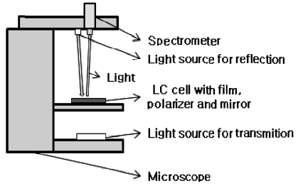
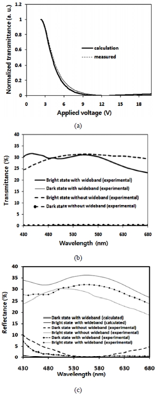
The optical characteristics of the fabricated cell were measured using a spectrometer (MCPD-3000, Photal) and a microscope (Nikon ECLIPSE E400 POL) with two white light sources (halogen lamps). Fig. 5 is the measurement system. In Fig. 6, we compared the experimental results with the calculated values in the proposed structure, and also the experimental results of wavelength dispersion in the transflective LCD with wideband structure and without it. Fig. 6(a) shows the electrooptic characteristics of the dynamic part. The bias voltage for the retention of the low bend state was 2.3 V and the transmittance of the fabricated LC cell was minimized by an applied voltage of 12 V. Although it showed a slightly different slope for the two curves, the measured results show a tendency similar to the calculated ones. We think that the deviation is caused by the mismatch of optical components of the LC cell created during the real fabrication process. So the measured results were not identical results with calculated ones. Fig. 6(b) shows the transmittances with respect to the wavelength with and without wideband structure in the transmissive dynamic mode. The dark states are perfectly compensated and both bright states have transmittances of over 25% in the whole visible range. Fig. 6(c) shows the reflectance dependence on the wavelength for the dark and bright states of the memory. In the reflectance measurement, the angle of incident light is about 5° and the reflectance is defined as the percentage ratio of the reflected intensity (brightness) by the LC cell divided by the reflected intensity by the mirror alone. For the splay state of the memory operation, a very low reflectance was obtained in the dark state and the reflectance of below 10% with respect to that of the bright state were obtained in the whole visible range due to its wideband structure. The bright state in memory mode, which is the π-twist state, also showed the reflectance of over 25% with respect to the power of the light source. Although the reflectance of the bright state was a little lower than the calculated value, the measured results show tendencies similar to the calculated ones. The light leakages of the splay state under the condition of the wideband structure were decreased by over 60% than those of the LC cell without wideband structure [3]. As a result, high contrast ratios of over 300:1 and 50:1 were achieved for the dynamic and memory parts, respectively.
In conclusion, we proposed a transflective configuration of a dual mode LCD having a wideband QWP structure for the reflective memory mode. The transmissive and reflective parts have a single cell-gap and single rubbing direction for the dynamic and memory mode operations, respectively. By optimizing the parameters of the LC cell and compensation films, a very low reflectance for the dark state and a high reflectance for the bright state in the memory mode were obtained, as well as a driving voltage of under 15 V for the dynamic mode. As a result, high contrast ratios of over 300:1 and 50:1 for the dynamic and memory modes, respectively, could be achieved.