In this work, a numerical analysis of a CIGS (CuIn1-xGaxSe2) solar cell with a rectangular grating onthe electrode is presented. The effects of the grating on the energy conversion efficiency are calculatedusing the RCWA (rigorous coupled wave analysis) method. In conventional CIGS solar cells, the thicknessof the light absorption layer (CIGS) is 2 ㎛, at which the incident light is almost absorbed. By adoptinga grating on the electrode and using a less than 1 ㎛ CIGS layer, we obtained a higher efficiency comparedto the conventional solar cells.
Recently, solar cells have gained significant interest due to their environmentally friendly technology. There are several semiconductor materials for converting light power into electricity such as c-Si (crystalline Si), GaAs, CdTe, CIGS(CuInGaSe), etc. c-Si has been the most popular material for solar cells because its high internal quantum efficiency due to its crystalline structure gives the highest energy conversion efficiency achieved to date. However, by its indirect bandgap, Si has a poor light absorption efficiency, making it necessary to make the thickness of Si to be on the order of several hundred micrometers. This has been a roadblock preventing c-Si solar cell use in office buildings and as a home electric power source due to its high manufacturing cost. Reducing the thickness of the thin film solar cell is a promising technology for saving on expensive semiconductor materials and decreasing the process time. Among various thin film technologies, amorphous Si (a-Si) is a strong candidate for replacing c-Si because there are tremendous technical achievements in the LCD (liquid crystal display) technology due to factors such as a very low cost, mass production, and large scale processing of a-Si as an active device. But, a-Si has light absorption characteristics similar to those of c-Si. Besides, a-Si has very low internal quantum efficiency due to its amorphous structure. To enhance the absorption of the light, several light trapping methods such as nano-scale structure, gratings, and surface texturing have been developed [1-3]. Even if the light trapping methods show successful improvements in the energy efficiency of an a-Si solar cell, the efficiency is less than 10% at the research level, and it is about 4-5% at the production level.
For CIGS solar cells, an active layer thickness below 2 μm is of great interest, and due to its high optical absorbing property over hundreds times more than Si, CIGS is a promising candidate for the next generation thin film solar cell [4-7]. In this paper, a grating structure is proposed to reduce the active layer thickness to a level less than 1 μm and we show the enhanced light absorbing characteristics compared to the conventional structure. RCWA algorithm [8] is used to calculate the amount of the absorbed, reflected and transmitted light at the solar cell. Finally, the energy conversion efficiency is calculated by using the well-established characteristic equation for CIGS material [7].
II. STRUCTURE OF CIGS SOLAR CELL
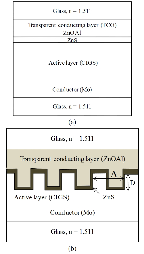
The common structure of CIGS solar cell [4] is depicted in Fig. 1 (a).
The refractive index and absorption coefficient of the CIGS according to wavelength are obtained from Ref [5], and the mole fraction x in CuIn1-xGaxSe2 is set to 0.3, which is the general case in most CIGS solar cells. For conventional CIGS solar cells, the thickness and refractive index for each layer are listed in table 1
As shown in fig. 1(a), the incident lights travel into the light absorbing layer (CIGS) without any loss. Inside CIGS layer, the light is absorbed and changed into electron-hole pairs, and the electron goes up to the upper conductor layer (TCO), at the same time, the hole goes down to the Mo layer. By these processes, the light energy is changed into electrical power. The light from the sun consists of nearly parallel rays with random polarizations. When the light enters the solar cell normal to the surface, then the travel length of the light in the CIGS layer is only 2 μm. If the light can be diffracted at angles with respect to the layer surface, the travel length of the light in the CIGS will be increased over several micro meters, and hence, more light is absorbed with less thickness of CIGS, for example, 1 μm. This can be achieved in the proposed
[TABLE 1.] Material parameters for CIGS solar cell
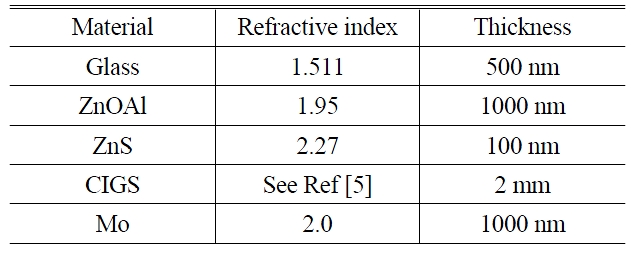
Material parameters for CIGS solar cell
structure in fig. 1 (b). The grating in the TCO and ZnS diffracts makes the incident light into the active (light absorbing) layer. The optimum period and depth of the grating can be determined by finding through simulation the best energy conversion efficiency considering the limit of the capable semiconductor fabrication process. The equation for energy conversion efficiency of the CIGS layer which converts the incident light into electrical energy is well explained in ref [7].
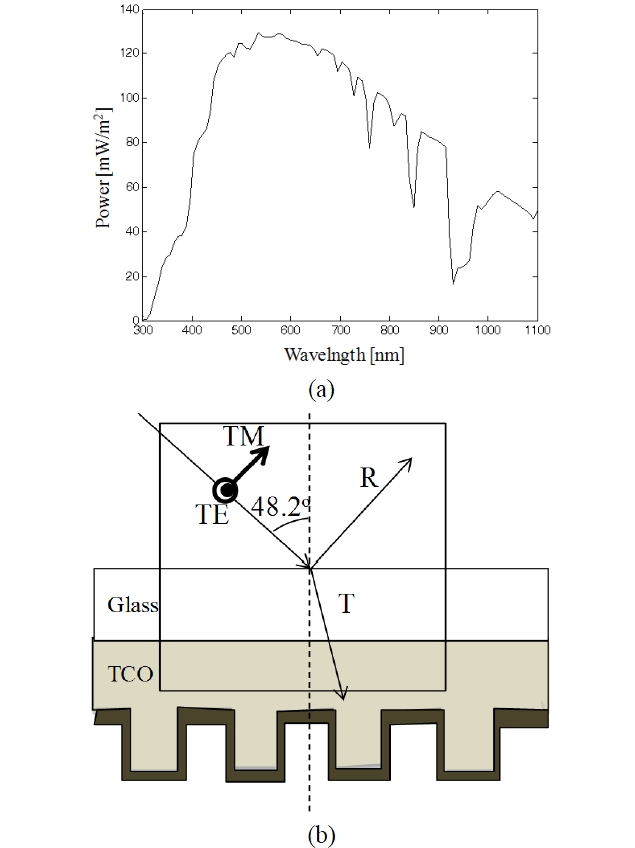
In the field of solar cells, the light from the Sun is generally modeled by the Air Mass model (AM) which considers the atmosphere of the Earth. Especially, in the mid-latitudes, AM 1.5 is used as a standard sunlight model as shown in fig. 2 (a). In AM 1.5, the wavelength covers at least from 300nm to 1100nm, and the light is incident upon the surface of the Earth (or a solar cell installed parallel with the Earth) with an angle of 48.2°. In fig. 2 (b), the light is divided into two orthogonal polarized, TE and TM modes with 50:50 power ratios due to the random polarization nature of the light through the atmosphere from the Sun.
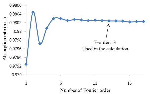
In the simulation presented in this paper, the internal quantum efficiency of CIGS material is set to 100% because only the effect of the grating on the CIGS thickness reduction and the energy efficiency are considered. The 3-dimensional RCWA algorithm is used and computed by the parallel computing method built in MATLAB which is a well-known engineering programming software. In RCWA, the accuracy is determined by the Fourier orders used in the calculation. Fig. 3 shows the absorption rate when F-order (Fourier order) varies from 1 to 18. The period and depth of the grating in this case are 1100nm and 400 nm, respectively. The absorption rate is nearly unchanged when F-order is over 10. Therefore, in the simulation, F-order 13 is used.
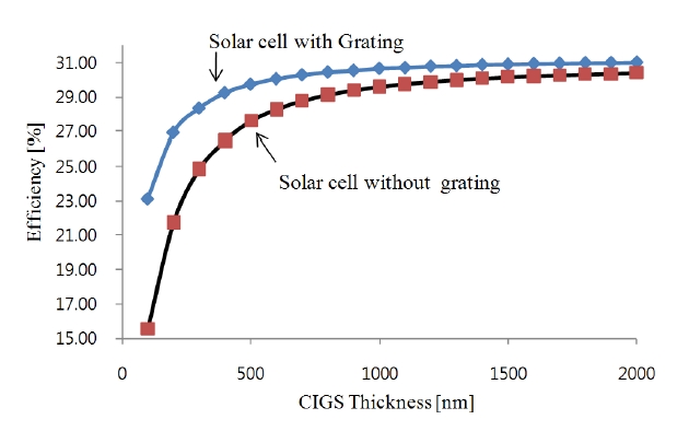
Fig. 4 shows the simulation results for the solar cells with the grating and without the grating. The period and depth of the grating are the same as those of fig. 3. In the simulation, to separate the effect of the thickness of the active layer, the absorption coefficient of the CIGS material in the portion of the grating, which is inside the ‘D’ portion in fig. 1(b), is neglected. Therefore, the CIGS in the ‘D’ portion is not the active material, and only is considered as a dielectric material. If CIGS in the ‘D’ portion is considered as an active material, the efficiencies of the solar cells with grating will be higher than those in fig. 4.
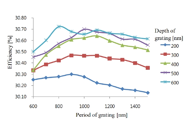
In fig. 4, the effect of the grating on the efficiency enhancement is verified. The thinner CIGS solar cell shows a great improvement in efficiency. The efficiency of CIGS with thickness of 2 μm with planar structure is 30.40%, whereas, that of the grating structure of CIGS with 1 μm thickness is 30.64%. The energy conversion efficiencies for the various grating periods and depths are shown in Fig. 5. The best energy conversion efficiency is 30.72% when the period and depth are 800 nm and 600 nm, respectively. Without the grating, the efficiency is 29.61 when the CIGS thickness is 1 μm. With the CIGS thickness of 2 μm, the efficiency is 30.40% which is still 0.32% lower value compared to the solar cell with the grating structure. According to the simulation results, we can conclude that the CIGS solar cell with the grating can have very thin active layer less than 1 μm, and hence, it is possible to reduce the amount of expensive semiconductor materials and the process time.
In this paper, the effect of the grating on the energy efficiency of the CIGS solar cell is verified by the simulationof a well-known RCWA algorithm. By adopting thegrating structure inside the solar cell, the thickness of theactive layer, which is made of very expensive semiconductormaterials, can be made to be less than 1 ㎛without any loss of energy conversion efficiency.