Mankind has utilized electromagnetic (EM) waves, including optical waves, throughout history. Each region of their wide spectrum has its own applications - optical and wireless communications, lighting, optical lithography[1, 2], radio and television broadcasting, sterilization of medical equipment, detection of many physical quantities, diagnosis of problems of the human body, to name a few. Most of today’s advanced technologies employ EM waves. For each application of EM waves, appropriate wave sources have been developed. For example, modern optical networks having huge transmission capacity could not have been realized if it had not been for compact infrared semiconductor lasers [3].
Recently there has been much interest in the THz region[4-6] a relatively unexplored region of EM waves. This region is located between 0.3 and 10 THz in frequency, or equivalently, between 30 and 1000 ㎛ in wavelength. Despite great applicability to examining living tissues like human cells, there is no THz source which is compact and easy to use.
As an effort to resolve such a problem, in this work, we have developed a microcolumn that can be used as a convenient source module. There has been steady research in the microcolumns that can be used for microscopy and its applications. While the principle of the microcolumn is the same as that of conventional e-beam equipment, its structure can be simplified very much compared to that of the convential e-beam equipment due to the miniaturized electron lenses. The characteristics of microcolumns have shown the potential of microcolumns as widely tunable THz sources (including far infrared).
II. DEVELOPMENT OF THE MICROCOLUMN
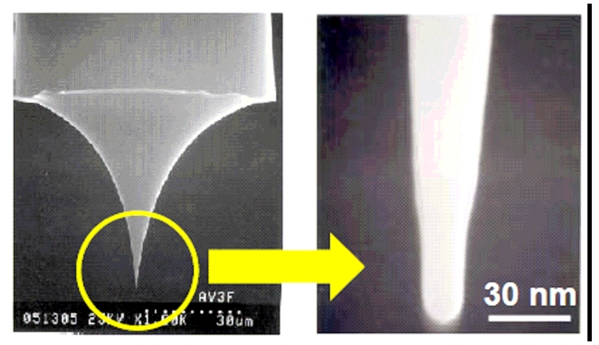
The microcolumn is composed of several elements including an electron emitter, a scan deflector, and electron lenses. Among these elements, the electron emitter is the source of the electron beam (e-beam), and its characteristics determine the whole performance of the system. In this work, we have fabricated a cold field emitter (CFE) having a very sharp tip by electro-chemically etching tungsten (W)[7]. In the conventional CFE that has been used in large-scale electron columns, the diameter of the tip is larger than 100 nm. With such a large radius of curvature, the tip cannot emit electrons unless the voltage bias applied to the tip is sufficiently high (typically higher than 10 kV).
Since such a high voltage causes physical damage to the micro-lenses of the microcolumn, we have developed a very sharp tip with diameter much less than 50 nm. Fig. 1 shows the scanning electron microscope (SEM) image of the tip we have developed. With this sharp tip, we could decrease the voltage bias to as low as -230 V.
The resolution of the microcolumn system is significantly influenced by aberrations such as astigmatism, coma, spherical aberration and chromatic aberration, which are, in turn, dependent on the eccentricity of the lens aperture and alignment of the system components. Two sets of lenses are required in the microcolumn. One is a source lens set that extracts the electrons from the emitter and controls the diameter of the e-beam. The other is an Einzel lens set which concentrates the e-beam around the target point of the sample that is being processed by the microcolumn system[8, 9]. Both source and Einzel lens sets were composed of three electron lenses in our microcolumns.
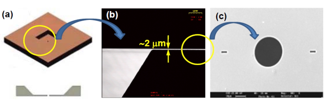
Each electron lens was fabricated by making a circular aperture in a 2-㎛ thick Si membrane through semiconductor processing technologies like lithography, cleaning, and dry etching. The size of the membrane was 2×2 mm2, and it was located at the center of a silicon chip whose dimension was 10×10 mm2. Fig. 2 is an SEM image of the electron lens. The diameter of the lens aperture was 200 ㎛.
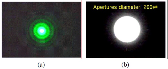
To investigate the shape of the lens aperture and the alignment of the lens assembly, we have used laser diffraction [10]. By illuminating each lens or lens assembly with a He-Ne laser, we have obtained the corresponding Fraunhofer diffraction pattern. When the aperture is a perfect circular disk, the intensity profile of the diffraction pattern follows the first-order Bessel function. Hence, by observing the diffraction pattern, we could select the electronic lenses having circular apertures.
We could also find the diameter of the aperture by combining the pattern data with the optical wavelength and the distance between the aperture and the diffraction pattern. This is a very precise and convenient method for measuring the size of the small circular hole. The lens assembly composed of several electronic lenses also shows the same diffraction pattern when they are in good alignment. We used this to adjust the position of the lenses in fabricating the microcolumn.
Fig. 3 shows (a) the diffraction pattern from two aligned Einzel lenses having 200-㎛ apertures and (b) top-view microscope image of the assembled lens set. From the circular diffraction patterns and the photograph, we could confirm that the eccentricity of the apertures was almost zero and the alignment of the lenses was very good.
III. CHARACTERISTICS OF THE MICROCOLUMN
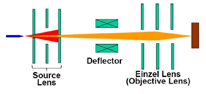
Fig. 4 is the experimental set-up for characterization of the microcolumn that we developed. In the figure, the set
of extractor, accelerator, and limiting aperture is called the source lens. Usually a negative bias is applied to the electron emitter and the source lens is grounded to extract the electrons from the sharp emitter tip. We have analyzed the characteristics of the microcolumn developed by measuring the e-beam currents at the first electron lens and at the sample with respect to the various bias voltages
The electron emitter was characterized at the UHV pressure of 5×10⁻¹⁰ torr. To accurately measure the e-beam current, we used a precision DC power supply that can provide 1-kV DC voltage while maintaining peak-to-peak fluctuation less than 10 mV. The e-beam currents were measured using a pico-ammeter at the first aperture (extractor), at the second aperture, and at the sample. We also observed the images of Cu grid sample(mesh 1000) by using the microcolumn as the electron microscope.
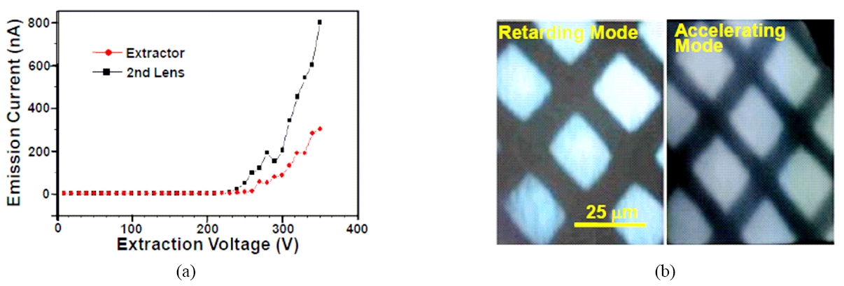
Fig. 5(a) shows the measured e-beam currents. The electron emission began at bias voltage as low as -230 V, which was a significant reduction compared to the -10 kV bias of the conventional electron column, proving that the diameter of the emitter tip was much less than that of the typical emitter tip. The effective diameter of the tip extracted from the Fowler-Nordheim plot[11] based on the I-V curve was found to be around 12 nm.
The e-beam currents at the first electron lens were 200 nA at the bias voltage of -300 V, and increased up to 800 nA at -350 V. The electron current at the sample at -300V bias was measured to be 0.25 nA, which meant that more than 0.1% of the emitted electrons reached the sample.
The Einzel lens was used to focus the electron beam by applying a retarding or an accelerating bias to the center electrode of the Einzel lens. The other two electrodes of the Einzel lens are usually grounded, and hence the energy of the electron beam arriving at the sample depends only on the potential applied to the emitter tip. The focused electrons coming from the Einzel lens can be used for lithography or for other applications like imaging.
To evaluate the performance of the microcolumn, the images of a Cu grid sample were captured for both retarding and accelerating modes. Fig. 5(b) shows the result. For the retarding mode, the grid pattern was distinguishable when the bias voltage applied to the Einzel lens was lower than -200 V and the clearest image was obtained at the bias voltage of -253 V. For accelerating mode, the biases for the distinguishable and clearest image were +850 V and +934 V, respectively. While the accelerating mode shows better resolution, which is expected theoretically, it requires higher voltage bias for concentration of the e-beam. Since the insulation layer between the electrodes is extremely thin in the microcolumn, the retarding-mode operation is preferred for long-time stability. The result proved that the electric current arriving at the sample was sufficiently large to use the microcolumn as an e-beam source.
We have developed an efficient e-beam source, a microcolumn, that can be used as a source module which covers THz and far infrared regions of the EM spectra. To achieve the low operating voltage, we developed a very sharp emitter tip by electrochemically etching a tungsten wire. The effective diameter of the tip estimated by Fowler-Nordheim plot was about 12 nm. To obtain a large current at the end of the microcolumn, high-quality electron lenses were fabricated and aligned very precisely by observing the laser diffraction patterns. More than 0.1% of the electrons emitted by the tip passed through the microcolumn, which made it possible to capture the SEM image of a Cu grid sample (mesh 1000) and confirmed the potential of the microcolumn as an electron source module.