Amorphous silicon thin film solar cells (a-Si TFSCs) are considered promising candidates for future low-cost and large-area photovoltaic devices. Light trapping is considered an essential mechanism that allows the reduction of reflection losses with an increase in the optical path length of incident light in photovoltaic devices. The front transparent conductive oxide (TCO) films must exhibit good transparency, low resistivity and excellent light scattering properties for high efficiency a-Si TFSCs. Various textured TCO films like SnO2:F, ZnO:Al, and ZnO:B are commonly used as substrates to increase the light path within the absorber layer for the enhancement of light trapping in the solar cell [1-15]. However, these textured TCOs substrates are insufficient to gain the light scattering effect needed for longer wavelength region due to their smaller (~600 nm) textured size features. Recently, few research groups proposed larger feature size TCO substrates. Arbitrary patterned glass substrates and self-assembled metal particle applying to etching mask [54].
An alternative approach to improve the light-trapping in a-Si TFSCs is to use of TCO films on the textured glass substrates [1-10]. Various methods to create textured glass surface morphologies have been investigated in recent years like sand blasting, powder blasting, wet chemical etching with hydrofluoric acid (HF) based solutions, aluminum induced texturization (AIT) and plasma etching through a nanostructured metal mask [11-16]. Thus, the textured glass surface substrates with nano- and micro size features can be employed to scatter light in lower as well as in longer wavelength region. Recently, textured glass surface morphologies with high rms roughness and haze ratio were proposed for high efficiency a-Si TFSCs due to their superior electrical and optical characteristics as compared to textured TCO films [15,16-25].
The inductive coupled plasma-reactive ion etching (ICP-RIE) process has received much attention, as the glass surface can be textured with high rms roughness and haze ratio. Hongsingthong et al. [6-8] reported the influence of RIE textured glass substrates with high rms roughness and haze ratio of ZnO films for the improved performance in a-Si TFSCs, due to their nano- and microsize textured surface morphologies. Isabella et al. [4] reported modulated surface morphologies with various geometrical features for an enhanced scattering mechanism.
These nano- and micro-size textured surface morphologies can scatter light in the visible as well as NIR wavelength regions [4,7-10]. Recently, Hussain et al. [5,39,54] reported the influence of periodic SF6/Ar plasma textured glass surface morphologies for the light trapping in a-Si TFSCs.
We review the relevant literature reports on plasma textured glass surface morphologies for a-Si TFSCs and various popular light scattering surface morphologies for the TCO films are discussed. A short historical survey of textured glass surface morphologies for amorphous silicon solar cells is included in this review. Several RIE textured glass surface morphologies with various experimental parameters are also discussed.
2.1 Textured TCO surface morphologies
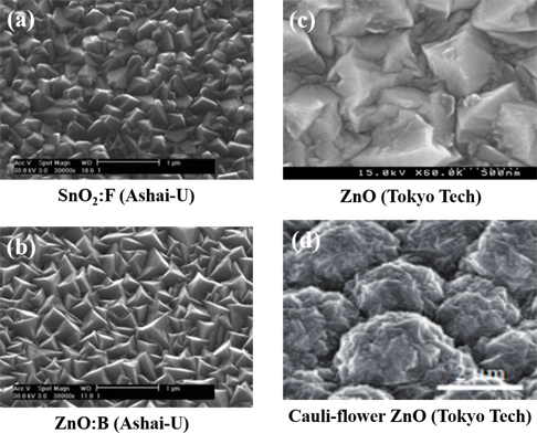
Rough TCO/silicon interfaces are generally used in a-Si TFSCs for an efficient light trapping. Effective light scattering not only enhances the current density of a-Si TFSCs but also saves cost by making thinner solar cells [26-40]. To obtain textured TCO surface morphologies, various strategies have been applied in the solar cell industry. Figure 1 shows various light trapping surface morphologies for the TCO films. Figure 1(a) and 1(b) represents textured TCO surface morphologies of SnO2:F and ZnO:B films being employed by the Ashai-U research group [46,56-61]. The ZnO:B films were grown by low pressure CVD (LP-CVD) from precursors of diethyl-zinc and H2O; the conductivity was easily controlled by using di-borane as the dopant source [58,59]. The SnO2:F were deposited by (APCVD) from the precursors of SnCl4 and H2O [60-62]. Figure 1(c) and 1(d) show pyramid and cauliflower ZnO surface morphologies used by Tokyo technology. The pyramid type ZnO films were deposited on the Corning glass substrate by MOCVD technique by using D2O and H2O mixtures as oxidants for di-ethylzinc (DEZ). A mixture of D2O/H2O was employed to control the surface morphology of the ZnO films [1,6,7]. The cauliflower ZnO films were deposited on RIE textured glass substrate using a MOCVD process with a mixture of D2O/H2O for the control of surface morphology [6]. B2H6 (1% H2 diluted) was used as the dopant gas. Photovoltaics laboratory (PV-Lab) is well known for the various light trapping techniques employed in a-Si TFSCs. The ZnO:B films used by PV-Lab are deposited by low pressure chemical vapor deposition (LP-CVD) process for the light scattering in a-Si TFSCs [59,63].
2.2 Plasma textured glass surface morphologies
Plasma etching (physical sputtering) was introduced to integrated circuit (IC) manufacturing in the 1970s to reduce liquid waste disposal in manufacturing and achieve high selectivities as compared to wet chemistry. The ability to anisotropically etch aluminum, silicon, and silicon dioxide in plasmas became the innovation that allowed the features in IC technology to continuously shrink over the next 40 years. Today, plasma etching plays a major role in allowing complex circuit patterns printed in a photolithographically deflned polymers to be transferred to the glass, silicon, metals and silicon dioxide that make up the integrated circuits at the heart of these devices [10,41-44,64].
Silicate glasses are widely used in everyday life due to their unique properties. Silicate glasses are generally resistant to most gases and liquids and at room temperature they are only readily dissolved by hydrofluoric acid or other HF containing aqueous solutions. These glasses are used for variety of applications with controlled dissolution in HF-based etchants [44-47,65].
Commonly used plasma parameters for the ICP-RIE system are flow rate of etching gas, etching time, RF power, biased power and the pressure. Here, we include few experimental results of RIE textured glass surface morphologies [21-24]. Various etching chemistries are generally used for glass etching. Commonly used etching chemistries contain CF4 [6,7,11,38] and SF6 [5,39,55] gases with the addition of either O2 or Ar for the glass etching. Few research groups also used CHF3 etching gas to texture glass. Konagai et al. mostly employed CF4 gas for the random texturing of glass surface morphologies. Various metal masks like Al, SiN3, and PR are used for etching purposes according to the applications [48-50].
Table 1 illustrates the short historical survey about the textured glass surface morphologies used for solar cells. Most of research groups used Corning 7059 or Corning XG glass as a substrate due to their chemical composition. CF4 and SF6/Ar are the commonly used etching gases for the texturing process. High rms roughness, transmittance and haze ratio are preferred characteristics for the a-Si:H or μc-Si:H solar cells. Most of the researchers used randomly textured RIE glass surface morphologies for the TCO deposition. The hot debate between random or periodic textured surface morphologies being superior for light trapping and high value of current density is under investigation [5-10,39,55]. Few research reports of periodic textured ICP-RIE glass surface morphologies for solar cell applications are recently available [5,39,55].
[Table 1.] Various plasma textured glass surface morphologies for solar cell applications.
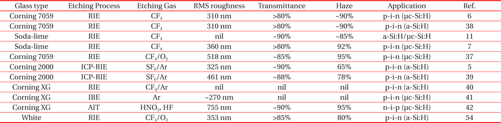
Various plasma textured glass surface morphologies for solar cell applications.
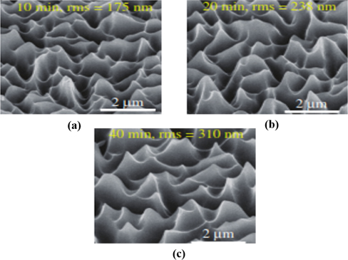
Figure 2 represent textured glass surface morphologies with various glass-substrate treatment times. The rms roughness of each surface morphology was obtained from 3-D AFM images (scan area: 10 μm × 10 μm). As the glass substrate treatment times increased from 0 min to 40 min, the surface of the textured glass surface morphology changed from flat to largely textured. The rms roughness of the glass substrates increased from 1.27 nm to 175 nm as the treatment time increased from 0 min to 10 min. With the further increase in treatment time from 10 min to 40 min, the rms roughness of glass surface morphology increased from 175nm to 310 nm, respectively [6,24,25].
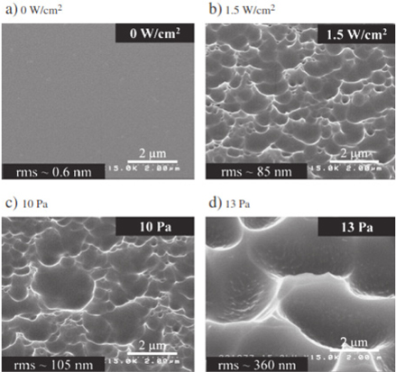
The SEM images and rms roughness of the surface of sodalime glasses with various etching conditions are shown in Fig. 3. As the power density was increased from 0 W/cm2 to 1.5 W/cm2, the glass surface changed from a smooth flat surface to one with small craters and lateral feature size of 200 nm to 700 nm. The textured glass surface became smoother when the power density was 1.9 W/cm2 with rms value of 3 nm. This may be due to the difference in the energetic ion bombardments [7,51] that affect the etching kineticd and allow smooth surfaces. The rms roughness of textured glass slightly increased as the power density increased to 1.5 W/cm2, and showed a quick drop for power densities greater than 1.5 W/cm2. Figure 3(c) and 3(d) represent textured soda-lime glass surface morphology with varying pressures. The textured soda-lime glass surface morphology changed from a flat surface to one with large craters and lateral feature sizes between 4,000 nm and 6,000 nm, as well as having rms roughness increase from 0.6 nm to 360 nm with the increase of gas pressure from 0 Pa to 13 Pa. The different surface textures at various gas pressures may be caused by the variation of gas radical concentrations like ion-radical and neutral etchant species in the dry plasma [7,50,51].
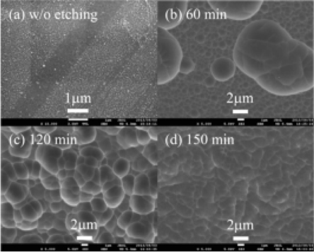
Figure 4 shows the textured glass surface morphologies for various RIE etching times. The surface of white glass was etched gradually with the etching time up to 60 min. However, large crater sizes suddenly appeared on the glass surface. Various craters sizes ranging from 1 μm - 10 μm) were identified on the textured glass surface. The glass etching rate with CHF3-CF4 mixture gas can be decreased with increasing nonvolatile elements contents in glass surface morphology as reported by Leech [54,66]. Thus, the area with low and high etching rates appeared due to the segregation of silica and nonvolatile elements that exist on the glass surface [11,52,53]. As the etching time increased from 60 min to 120 min, crater feature size became constant at an approximate size of 4 μm. With the increase of etching time of about 150 min, the glass surface was dominated by smaller craters. The silica and nonvolatile element compositions at the inner part of glass stabilized. The chemical etching mechanism of CF4/O2 for RIE process is given as,


Where the SiF4, O, and CO are volatile compounds and were evacuated from the chamber immediately [54].
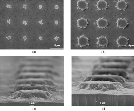
Figure 5 shows the SF6/Ar plasma textured glass surface morphologies with various UV photo-lithography pattern dimensions. The glass with pattern dimensions of (6×6) and (12×5) μm2 were etched to (3×9) and (8×9) μm2 after 60 min of ICP-RIE process as shown by Fig. 5(a) and 5(c). The Al under-cut was primarily related to chemical etching and micro-trenching that increases with the passage of time. The Ar was mixed with SF6 gas to remove under-cut and micro trench formation by the fast removal of by-products. Figure 5(b) and 5(d) shows the crosssectional views of the SF6/Ar plasma textured glass surface morphologies. All the textured glass surface morphologies showed almost uniform etching rate due to the fixed ICP-RIE process conditions. The minor variation in the etching rate from 22.66 nm/min to 27.33 nm/min was related to the different surface structure of glass. The maximum etching depth of ~ 1.73 μm was recorded by the textured glass with the pattern dimension of (12×5) μm2. The higher concentration of metal elements like F, B, Al and Na in the glass surface can reduce the etching rate of textured glass by ICP-RIE process. These metal elements produced the non-volatile etch products after reacting with halogen gases. The Ar gas can be used to remove the non-volatile etch products by physical etching [5,39,55,66,67]. The etching mechanism of SF6/Ar is readily available in following research reports related to textured glass [5,39,55,68].
Front TCO films have the important role of enhancing the current density and hence improve the performance of a-Si TFSCs. An alternate approach for improved light trapping surface morphology is to texture the glass substrate instead of the TCO films. We present various plasma textured glass surface morphologies for light trapping in a-Si TFSCs. RIE is an important process to texture the glass surface with precise accuracy. RIE textured glass surface morphologies contain the micro- and nano-size features that can enhance the light scattering in visible as well as in NIR region. ICP-RIE textured glass surface morphology with high rms roughness, haze ratio are also proposed for the future high efficiency a-Si TFSCs.
![Various light trapping surface morphologies for the transparent conductive oxides (TCOs) films. Fig. 1 (a), (b) are reproduced with permission from [46], F. -J. Haug et al., Light management in thin fllm silicon solar cells, Energy Environ. Sci.,8 (2015) 824. Permission granted. License number 3679260160905 Copyrightⓒ Royal Society of Chemistry. Fig. 1 (c) is reproduced with permission from [1], M. Konagai, Present Status and Future Prospects of Silicon Thin-Film Solar Cells, Jpn. J. Appl. Phys. 50 (2011) 030001. Permission granted Copyright ⓒ The Japan Society of Applied Physics. Fig. 1 (d) is reproduced with permission from [6], A. Hongsingthong et al., ZnO Films with Very High Haze Value for Use as Front Transparent Conductive Oxide Films in Thin-Film Silicon Solar Cells, Appl. Phys. Exp.,3 (2010) 051102. Permission granted.Copyrightⓒ The Japan society of Applied Physics.](http://oak.go.kr/repository/journal/20769/E1TEAO_2016_v17n2_98_f001.jpg)

![SEM images of textured glass substrates for various etching times. The rms roughness of each textured glass is also shown. Reproduced with permission from [6], A. Hongsingthong et al., ZnO Films with Very High Haze Value for Use as Front Transparent Conductive Oxide Films in Thin-Film Silicon Solar Cells, Appl. Phys. Exp., 3 (2010) 051102. Permission granted. Copyright ⓒ The Japan society of Applied Physics.](http://oak.go.kr/repository/journal/20769/E1TEAO_2016_v17n2_98_f002.jpg)
![SEM micrographs of soda-lime glasses with various etching conditions: a) 0 W/cm2; b) 1.5 W/cm2; c) 10 Pa; and d) 13 Pa. Reproduced with permission from [7], A. Hongsingthong et al., Development of textured ZnO-coated low-cost glass substrate with very high haze ratio for silicon-based thin fllm solar cells, Thin Solid Films, 537, (2013) 291. Permission granted. Copyright ⓒ 2013 Elsevier.](http://oak.go.kr/repository/journal/20769/E1TEAO_2016_v17n2_98_f003.jpg)
![SEM micrographs of RIE-etched white glass substrate under various glass etching times: (a) no etching; (b) 60 min; (c) 120 min; and (d) 150 min. Reproduced with permission from [54], H. Wada et al., Improved light trapping effect for thin-fllm silicon solar cells fabricated on double-textured white glass substrate, Can. J. Phys., 92, (2014) 920. Permission granted. License number 3681950779704. Copyright ⓒ 2014 NRC Research Press.](http://oak.go.kr/repository/journal/20769/E1TEAO_2016_v17n2_98_f004.jpg)


![SEM images (top and cross sectional view) of the ICP-RIE textured corning glass with various pattern sizes. Reproduced with permission from [5], S. Q. Hussain et al., Light trapping scheme of ICP-RIE glass texturing by SF6/Ar plasma for high haze ratio, Vacuum, 94, (2013) 87. Permission granted. License number 3679461402631. Copyright ⓒ 2013 Elsevier.](http://oak.go.kr/repository/journal/20769/E1TEAO_2016_v17n2_98_f005.jpg)