검색 전체 메뉴
PDF
맨 위로
OA 학술지
A Short Wavelength Coplanar Waveguide Employing Periodic 3D Coupling Structures on Silicon Substrate
  • 비영리 CC BY-NC
  • 비영리 CC BY-NC
ABSTRACT
A Short Wavelength Coplanar Waveguide Employing Periodic 3D Coupling Structures on Silicon Substrate
KEYWORD
Short wavelength , Coplanar waveguide , Coupling structure , Silicon substrate , Impedance transformer
  • 1. INTRODUCTION

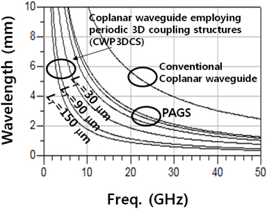
    For a miniaturization of wireless communication systems, onchip RF passive components should be realized on semiconducting substrates [1-3]. Until now, passive components employing conventional transmission lines have been fabricated outside of ICs due to their large sizes [4-12]. In order to solve this problem, transmission lines employing slow-wave structure have been developed [1-9]. Of all slow-wave structures, the coplanar waveguide employing periodically arrayed ground strip (PAGS) showed a much shorter wavelength compared with conventional coplanar waveguides [1-3]. At 10 GHz, the wavelength of the PAGS was 4.95 mm, which is 48.5% of conventional transmission line on silicon substrates [1-3]. However, this values is still too large for an integration of passive components on silicon substrate. For example, if an impedance transformer employing PAGS with an operation frequency of 10 GHz is fabricated on silicon substrate, its length is 1.24 mm, which is too long for an integration on silicon substrates. Therefore, integration of passive components on silicon substrates requires further reduction of wavelength [1-3].

    In this work, in order to realize a further reduction of wavelength, we developed a coplanar waveguide employing periodic 3D coupling structures (CWP3DCS) on silicon substrates. Of all slow-wave structures that have been reported to date, the CWP3DCS structure shows the shortest wavelength, being only 17.3% of conventional coplanar waveguides and only 35.6% of the transmission line employing PAGS structure. Using the CWP3DCS, a highly miniaturized on-chip impedance transformer was developed on a silicon substrate. The size of the impedance transformer employing the CWP3DCS on silicon substrate was 0.04 mm2, which was only 0.74% of conventional designs fabricated on silicon substrates.

    2. A NOVEL COPLANAR WAVEGUIDE EMPLOYING PERIODIC 3D COUPLING STRUCTURES ON SILICON SUBSTRATE

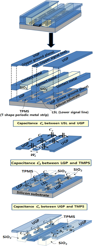
    Figure 1 shows the schematic design of CWP3DCS, showing comb-type lines on the silicon substrate. The fabrication process is described as follows. For the purpose of forming lower ground planes (LGP), lower signal line (LSL) and T-shape periodic metal strips (TPMS), a Ti/Au bilayer was deposited on silicon substrate by evaporation, then the contact metal was deposited by gold electroplating in a thick photoresist mold. After the formation of contact metal, 1 μm-thick SiO2 layer was deposited. Finally, Au was deposited to form the upper ground plane (UGP) and upper signal line (USL).

    The comb-type line consists of LSL and TPMSs, and the TPMSs are connected to the both sides of the LSL. The LGPs are placed on both sides of the comb-type line. USL and UGP exist on the top side of the novel coplanar waveguide structure. The USL is electrically connected to LSL through the contact metal, while UGP is electrically connected to LGP. The SiO2 film is placed between UGP and TPMS. Conventional coplanar waveguide has only a periodical capacitance Ca (Ca is shown in Fig. 1) between USL and UGP. Due to tight electromagnetic coupling between UGP and TPMS, the CWP3DCS has capacitance Cu as well as Ca. In addition, it has an additional the structure also has capacitance CS due to an electromagnetic coupling between LGP and TPMS.

    Figure 2 shows the wavelength of transmission lines on silicon substrate, showing wavelength (λg) to be much shorter than conventional transmission lines on silicon substrate because wavelength is inversely proportion to the periodical capacitance of transmission lines , λg = 1/[f·(LC)0.5]. In Fig. 2, spacing ST between TPMSs and line width WL, shown in Fig. 1, are all 20 μm, and width WT of TPMS and the thickness of SiO2 film are 26 μm and 1 μm, respectively. The length LT of TPMS (LT is shown in Figure 1) is a range of 30 μm ~ 150 μm. The thickness of silicon substrate is 600 μm. In previous reports [1-3], coplanar waveguides employing periodically arrayed ground strip (PAGS) were proposed, showing a much shorter wavelength compared to conventional coplanar waveguides. The CWP3DCS has various 3D capacitive couplings between signal lines and grounds as shown in Figure 1, which enables a further reduction of wavelength due to an increase of periodical capacitance. The periodic shunt capacitance of the conventional coplanar waveguide and PAGS structure were measured to be 0.14 pF/mm and 0.65 pF/mm, respectively, while the periodic shunt capacitance of the CWP3DCS was 8.15 pF/mm. At 10 GHz, the wavelength of the CWP3DCS with 150 μm of LT and conventional coplanar waveguide was 1.76 mm and 10.2 mm, respectively, and the coplanar waveguide employing PAGS structure was 4.95 mm. Therefore, the wavelength of the CWP3DCS is only 17.3% of conventional coplanar waveguide, and only 35.6% of the coplanar waveguide employing PAGS structure.

    3. A HIGHLY MINIATURIZED IMPEDANCE TRANSFORMER EMPLOYING THE CWP3DCS

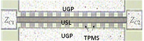
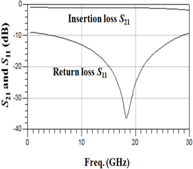
    Using the CWP3DCS, an on-chip impedance transformer was fabricated on silicon substrate. Figure 3 shows a photograph of the λ/4 transformer on silicon substrate. T-shape structure of the TPMS is hidden by the UGP. In this work, the source impedance (Zc1) and load impedance (Zc2) are 22.5 Ω and 10 Ω, respectively, and the characteristic impedance (Z0) of the transformer is 15 Ω. For a Z0 of 15 Ω, LT is 30 μm. In order to operate in a center frequency of 18.3 GHz, the length of the λ/4 transformer is 0.5 mm, and the total width of the transformer including line and TMPS is 80 μm. The size of the transformer employing the CWP3DCS is 0.04 mm2, which is 0.74% of the size of the transformer employing conventional coplanar waveguides [13] on silicon substrate, because the line width and length of the impedance transformer employing conventional coplanar waveguide on silicon substrate are 3 mm and 1.8 mm, respectively. If the impedance transformer employing PAGS is fabricated on silicon substrate, the size is 0.069 mm2. Therefore, using CWP3DCS enables further size reduction of RF circuit, because the CWP3DCS structure shows the wavelength to be much shorter than conventional transmission lines. Of all slow-wave structures that have been reported to date, the CWP3DCS structure showed the shortest wavelength.

    Measured return loss S11 and insertion loss S21 of the impedance transformer employing the CWP3DCS are shown in Fig. 4. The impedance transformer exhibits good RF performances in a wide frequency range and demonstrates return loss values better than -10 dB from 4.6 GHz to 28.6 GHz with insertion loss values better than -1.3 dB in the same frequency range. The impedance transformer shows a return loss of -36.5 dB and an insertion loss of -1.07 dB at a center frequency of 18.3 GHz.

    The impedance transformer showed the operation band of DC - 30 GHz. This result (DC - 30 GHz) is only a bandwidth for application to an impedance transformer. However, the actual bandwidth is a passband when the proposed structure is used for application to transmission line Therefore, using transmission line theory [13], we extracted the actual bandwidth of the CWP3DCS using the proposed structure in Figure 1 to theoretically characterize use of a simple equivalent shunt circuit [13]. According to the results, we can obtain the following passband equation:

    image
    image
    image
    image

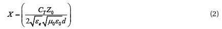
    In the above equation, εe and Z0 is effective permittivity and characteristic impedance of the transmission line without periodic structure, respectively, and μ0 and ε0 are permeability and permittivity of air, respectively, and ω and d is angular frequency and the length of unit cell of periodic structure, respectively. The above equations can be used to obtain the bandwidth of the CWP3DCS structure, which is 297 GHz and indicates feasibility in application as a transmission line in millimeter wave as well as microwave frequency.

    4. CONCLUSIONS

    We developed a short wavelength CWP3DCS on a silicon substrate. This CWP3DCS showed the shortest wavelength of all silicon-based transmission line structures that have been reported to date, which was only 17.3% of the wavelength of a conventional coplanar waveguide on silicon substrate. We fabricated a highly miniaturized impedance transformer employing the CWP3DCS on silicon substrate. The impedance transformer showed return loss values better than -10 dB in a broad band from 4.6 GHz to 28.6 GHz, and insertion loss values better than -1.3 dB in the same frequency range. The size of the transformer was 0.04 mm2, which was 0.74 % of the size of the transformer employing conventional coplanar waveguide on silicon substrate.

참고문헌
  • 1. Yun Y. (2011) [ETRI Journal] Vol.33 P.13
  • 2. Yun Y. (2010) [Microwave Journal] Vol.53 P.76
  • 3. Yun Y., Park Y. B., Park K. H. (2009) [IET Electronics Letters] Vol.45 P.270
  • 4. Kim C. S., Park J. S., Ahn D., Lim J. B. (2001) [IEEE Microwave Guided Wave Lett.] Vol.10 P.131
  • 5. Ahn D., Park J. S., Kim C. S., Kim J., Qian Y., Itoh T. (2001) [IEEE Trans. Microwave Theory Tech.] Vol.49 P.86
  • 6. Yang F. R., Ma K. P., Qian Y., Itoh T. (1999) [IEEE Trans. Microwave Theory Tech.] Vol.47 P.1509
  • 7. Andrenko A. S., Ikeda Y., Ishida O. (2002) [Microwave Opt. Tech. Lett.] Vol.32 P.340
  • 8. Lai A., Itoh T. 2005 [Proc. Asia-Pacific Microwave Conf.] P.31
  • 9. Gao J., Zhu L. 2005 [Proc. Asia-Pacific Microwave Conf.] P.39
  • 10. Cheung T.S.D., Long J. R. (2006) [IEEE Journal of Solid-State Cicuits] Vol.41 P.1183
  • 11. Chonhcheawchamnam M., Siripon N., Robertson I. D. (2001) [Electron. Lett.] Vol.37 P.501
  • 12. Fujii T., Ohta I., Kawai T., Kokubo Y. (2007) [IEICE Trans. Electron.] Vol.E90-C P.2245
  • 13. Pozar D. M. 1990 Microwave engineering google
OAK XML 통계
이미지 / 테이블
  • [ Fig. 1. ]  The coplanar waveguide employing periodic 3D coupling structures (CWP3DCS) on silicon substrate.
    The coplanar waveguide employing periodic 3D coupling structures (CWP3DCS) on silicon substrate.
  • [ Fig. 2. ]  Measured wavelength of the CWP3DCS and conventional transmission lines on silicon substrate.
    Measured wavelength of the CWP3DCS and conventional transmission lines on silicon substrate.
  • [ Fig. 3. ]  A photograph of single section λ/4 impedance transformer employing CWP3DCS on silicon substrate.
    A photograph of single section λ/4 impedance transformer employing CWP3DCS on silicon substrate.
  • [ Fig. 4. ]  Measured insertion and return loss of the single section λ/4 impedance transformer employing CWP3DCS on silicon substrate.
    Measured insertion and return loss of the single section λ/4 impedance transformer employing CWP3DCS on silicon substrate.
  • [ ] 
  • [ ] 
  • [ ] 
  • [ ] 
(우)06579 서울시 서초구 반포대로 201(반포동)
Tel. 02-537-6389 | Fax. 02-590-0571 | 문의 : oak2014@korea.kr
Copyright(c) National Library of Korea. All rights reserved.