Chemical sensors based on one-dimensional (1D) ZnO based nanostructures have attracted a great deal of attention because of their exquisite sensitivity and fast response to the surrounding environment [1-5]. In recent years, n-type and
Up to now, in room temperature operation, most of the gas sensors still face difficulties in getting a high response to the volatile organic chemicals (VOCs), such as ethanol, acetone, methanol and LPG. Furthermore, the study of the gas sensing properties of Ag doped ZnO NW to ethanol have shown room temperature operation for ethanol by using ZnO NWs [10]. In order to achieve high response and selectivity, different approaches, such as microstructure control, doping, or changing operating temperature, have been adopted to modify the sensing properties of semiconductor metal oxide gas sensors [11,12]. The sensing mechanism is known to be based on the surface reaction of the nanostructure with the exposed gas (adsorption and desorption of the test gas molecules. As adsorption is a surface effect, the adsorption of gas molecules can be increased by decorating the materials with nanoparticles or doping with an element with stronger chemical affinity for the particular gas molecule. Doping the NW can create defects which may play a role as preferential adsorption sites for gas molecules and help to sense pollutant gases at lower temperatures [13].
In this article, ZnO nanowires doped with 3 wt.% Ga and 3 wt.% Ag have been grown by using HW-PLD technology and nanowire gas sensors have been fabricated. The sensitivity ranges of ethanol gas sensors are varied, depending on the amount of Ga and Ag dopant due to different carrier concentration of the ZnO NWs. The ethanol gas sensing properties of these materials were characterized and discussed by using a self assembled sensing analyzer. The effect of Ag/Ga content on gas sensing properties to ethanol for high sensitivity and high selectivity was investigated in detail. The sensing mechanism of the gas sensor to ethanol was also discussed.
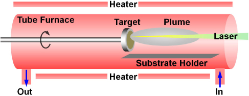
ZnO-based NWs were synthesized by HW-PLD process on a 20 Å Au film as a catalyst on sapphire substrates. HW-PLD has a target rotating system ensuring homogeneous target ablation. ZnO, 3GZO and 3SZO targets are used to fabricate the NWs under the optimized conditions. Pure ZnO, ZnO nanowires doped with 3 wt.% Ga (3GZO) and doped with 3 wt.% Ag (3SZO) have been grown by hot-walled pulse laser deposition (HW-PLD) technique. The diversed ZnO-based NWs were grown in HW-PLD furnace temperature of 800℃ with Ar carrier gas as shown in Fig. 1. During the deposition, Ar gas flow rate was fixed at 90 sccm and the pressure inside the quartz tube was maintained at 1.2 Torr by using in/out throughput. The morphology of as-grown samples was studied by field emission scanning electron microscopy (FE-SEM) operated at 20 kV. Energy-dispersive X-ray spectroscopy (EDX) analysis of a single NW was conducted to analyze the chemical composition of doped NWs. PL was carried out at low temperature (6K) with He-Cd laser at excitation wavelength of 248 nm. The energy density of the laser is set to 1.2 J/cm2 , and the area shot on the target surface is 0.042 cm2 . The growth time of ZnO-based NWs is 30 min.
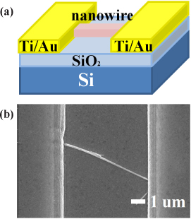
For the fabrication of the ZnO-based sensors, we spread NWs on Si substrates after cleaning. Soon after photolithography, the substrates were developed. For ohmic contact, metal electrodes consisted of Ti (20 nm) and Au (150 nm) were deposited by ebeam/thermal evaporator and patterned by a lift-off process to form contact pads on NWs. The sensitivity of the module is measured with the concentration of the ehtanol gas at 1 ppm in the self-designed gas chamber at 300℃.
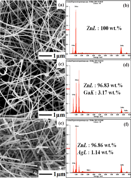
Figure 2(a)~(f) show the controlled morphology of the ZnO, 3GZO and 3SZO NWs and EDX spectra. SEM with EDX (SEM/EDX) is one of the electron probe microanalysis methods that have been used extensively to characterize the size, morphology, and elemental composition of the samples. The NWs have thread-like shapes and an Au nanoparticle at its end is clearly observed. It is understood that the nanoparticle is an Au catalyst that initiates the growth of the NWs by HW-PLD which is one of vapor-liquid-solid (VLS) mechanism. The catalyst can be identified based on the fact that the tips are brighter than the stem parts of the NWs. As can be seen in the figure, the orientation and the distribution of the NWs are random with the diameter of about 100 nm and the length of about 1 μm. ZnO based NWs were synthesized with ZnO targets by HW-PLD. Figure 2(a), (c), and (e) show the top view of FE-SEM images of ZnO-based NWs with pure ZnO, 3GZO and 3SZO with 20 Å Au film as catalyst. As shown in Fig. 2, lots of ramdom direction ZnO based NWs with a mean dimeter of abut 70 nm and an average length of about 9 μm were obtained at 800℃.
The EDX analysis yields reasonably accurate quantitative results featuring all the elements present in the tested compounds, namely, C, O, N, Na, S, Al, Si, and Cl. Furthermore, the carbon film has very low backscattered electron (BSE) yield compared to that from the particle. So in the BSE mode, the particle image can be observed with very high contrast. This improves quality and speed of the automated mapping of particles by SEM prior to EDX analysis [4]. Figure 2 is a backscatter electron image of the morphology and surface composition of the fractured surface of a specimen which are corresponding EDX spectrum. It is clearly observed ZnO, Ag and Ga in nanowires. The EDX spectrum revealed the presence of Zn, Ga, and Ag elements. HW-PLD is a well established growth method for oxide thin films and nanostructures of high structural quality. Therefore HW-PLD is a simple synthesis process and only target control can give an effective doping in the ZnO NWs. Such a result indicates that the impurities were doped well in the ZnO based NWs. According to the study in terms of Ag doping, it is considered that the irregularity of the heavily doped samples stems from the lattice stress induced by the substitution of Ag with Zn [5]. Unlike pure ZnO NWs, the 3SZO NW has many defects originating from the accumulated stress caused by the doping. Near the surface of the NW, many edge dislocations are found to support the doping-induced stress. NW growth direction is not perpendicular to the primary planes in forming the deviation from the upright ABABA stacking, implying a switch of the primary growth plane [6]. This means it is not easy to dope Ag with ZnO.
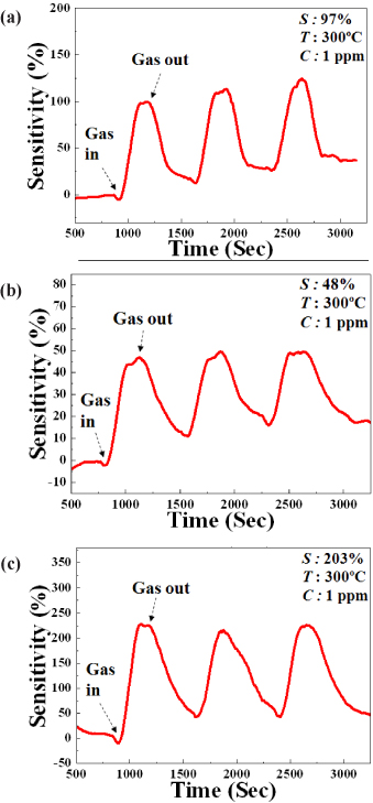
It is important to realize highly functional NW-field effect transistor (FET) devices for the purpose of the optimization of sensing properties and NW-FETs have lots of advantages to enhance the sensitivity and the selectivity for different gas species. It has been reported that ZnO NW-FET shows a remarkable n-type FET characteristics [14,15]. The transport properties of our single NW-FET device exhibited excellent n-type characteristics with strong gate control. The NW-FET sensors as shown in Fig. 3 were used for the detection of ethanol gas at 300℃. The system was purged with N2 gas to remove the excessive oxygen species from the surface on the NW in chamber. Comparison between the sensitivities of the ZnO, 3GZO and 3SZO NWs sensor for 1 ppm at 300℃ ethanol gas is shown in Fig. 4. The sensitivity which is defined as (Rg-Ra)/Ra, where
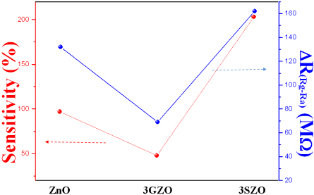
Figure 5 shows the relationship between the sensitivity and the resistance of various ZnO nanowires. As-grown ZnO nanostructures typically show n-type semiconductor due to intrinsic defects, such as oxygen vacancy and zinc interstitial. In contrast to n-type doping in ZnO materials,


In addition, the electrical detection of any chemical species is dependent on the surface reactions between the NWs and the chemical molecules. The ethanol sensing mechanism of this ZnO-based gas sensor can be described as follows [21]:

The gas response was demonstrated depending on the doping materials of ZnO NW-FET based sensors and the highest gas response (about 203%) was otained from 3SZO gas sensor. The sensitivity and sensing window of ZnO-based NW gas sensors can be expended by different doping in the NWs. The ZnO-based nanowres were fabricated by using a self-designed HW-PLD instrument to compare the sensing functions with various impurities same as reported before [22]. The conductivity and ethanol gas sensitivity of the sensors doped with different impurities were investigated. In the case of undoped ZnO, 3GZO and 3SZO NW gas sensor, measured sensitivities are 97%, 48%, and 203% when the sensor is operated at 300℃ for 1 ppm of ethanol gas. The response time and recovery time are also fair. Consequently, we can easily control the sensitivity on same gas by using different concentrations of Ga and Ag and selectivity is also expected to change with doping materials.
In summary, the gas response was demonstrated to be dependent on the doping materials of ZnO NW-based sensors, with the highest gas response (about 203%) otained from the 3SZO gas sensor. The sensitivity and sensing window of ZnO-based NW gas sensors can be expended by different doping of the NWs. The ZnO-based NWs were fabricated by a self-designed HW-PLD instrument to compare the sensing functions with various impurities. The conductivity and ethanol gas sensitivity of the sensors doped with different impurities were investigated. In the case of undoped ZnO, 3GZO and 3SZO NW gas sensor, measured sensitivities were 97%, 48%, and 203% when the sensor is operated at 300℃ for 1 ppm of ethanol gas. The response time and recovery time are also fair. Consequently, we can easily control the sensitivity of same gas by using different concentrations of Ga and Ag and selectivity is also expected to change with doping materials.
Doping of NWs can generate defects such as oxygen vacancies, metal interstitials, and surface defects which play vital roles in the sensing of ethanol gas. Experimental data confirm the prospects of thin ZnO NWs as active elements for nanoscale sensors operating at room temperature. These results demonstrate that ZnO NWs can be used as a gas sensing material for fabricating highly sensitive gas sensors for potentially wide applications in quick detection of poisonous and inflammable gases.