검색 전체 메뉴
PDF
맨 위로
OA 학술지
Properties of Defective Regions Observed by Photoluminescence Imaging for GaN-Based Light-Emitting Diode Epi-Wafers
  • 비영리 CC BY-NC
  • 비영리 CC BY-NC
ABSTRACT
Properties of Defective Regions Observed by Photoluminescence Imaging for GaN-Based Light-Emitting Diode Epi-Wafers
KEYWORD
Light-emitting diodes , Photoluminescence , Imaging , Optical inspection
  • I. INTRODUCTION

    In recent decades, high power light-emitting diodes (LEDs) based on III-V compound semiconductors have attracted attentions for their use in solid-state lighting and many other applications [1]. In the LED industry, the growth of nitride layers on heteromaterials, such as sapphire or silicon substrates, using metal-organic vapor phase epitaxy (MOVPE), has been considered as the most important process to obtain highquality blue and ultraviolet LED chips [2]. Therefore, the inspection of epi-wafers of LED structures obtained by MOVPE is essential to evaluate the epitaxial process and epi-layers before chip fabrication. Photoluminescence (PL) is currently the most widely used inspection method for LED materials. Particularly, PL mapping methods are employed in LED production lines, as they enable to analyze the uniformity of the epi-wafers and investigate various properties, such as wavelengths, intensity, half-widths, and epi-layer thickness, within a very short time [3]. However, as PL measurements are based on photo-excitation, which is different from the current injection operating LED chips, the estimation of optoelectronic properties at chip level using PL mapping results has been considerably difficult [4]. An electroluminescence (EL) mapping method, which inspects LED epi-wafers under current injection conditions, similar to those of the real LED chip operation, has been developed as an alternative technique [5]. Even though the EL mapping results showed better correlation with LED chip properties, a significantly longer inspection time than that of the PL measurements has hindered the adoption of the EL method for industrial purposes [5].

    We employed a PL imaging method to inspect a wide area of a GaN-based LED epi-wafer in a short time and obtain relevant information to estimate the LED chip properties. The PL imaging method for compound semiconductors was introduced by Livescu et al. in order to inspect a GaAs/AlGaAs p-i-n quantum well (QW) modulator structure and an InP:S substrate [6]. They obtained PL images of the compound semiconductor wafers using a CCD camera under various band-pass filtering conditions, with an expanded excitation laser beam exposing over a wafer. However, only few reports have been published on PL imaging of III-V compound semiconductor wafers, excluding the studies on spatial PL and cathodoluminescence (CL) imaging and mapping at the microscopic scale [7-9], whereas a lot of research has been recently performed on Si-based photovoltaic wafers and SiC wafers for defect recognition [10, 11].

    In this work, we analyzed the PL images of GaN-based QW LED epi-wafers. As the nitride materials of the active region have direct bandgap structures, images of the PL properties of that region could be directly obtained using a vision system. In the PL images, the defective regions of the active layer of the wafer appeared as dark spots with diameters in the range of ~ 50 - 1,000 μm. The dark spot defective regions (DSDRs) were analyzed by excitation power dependent PL measurements. Chip-wafers were fabricated from the epi-wafers whose PL images were acquired, and optical and electrical analyses of the LED chips were performed. The information on the defective regions obtained from the PL images was correlated with the optical and electrical properties of the LED chips.

    II. EXPERIMENTAL

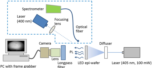
    Blue LED epi-wafers with InGaN/GaN multi-QW structures, grown on sapphire substrates by MOVPE, were examined using the PL imaging method based on a vision technology. To obtain the PL images, an experimental vision system as shown in Fig. 1 was assembled. The PL imaging setup was composed of a 405 nm laser as the excitation source, a diffuser for the expansion of the laser beam, a longpass filter for selecting a wavelength range of PL emission, a CMOS vision camera with a zoom lens, and a PC with a frame grabber. The diffused excitation laser beam was directed on the backside of the epi-wafers under inspection, while the camera recorded the images at the front side (epi-side) of the epi-wafers. A laser beam of 100 mW was diffused on the area to be inspected, which ranged from 0.5 to 20 cm2 depending on the optical quality of the epi-wafer. The diffused beam size was reduced to increase the excitation power density and make the defective area more distinguishable when the optical quality of the epi-wafer was relatively low. In this study, we employed a 425 nm longpass filter to prevent the transmitted excitation laser beam and to capture most of the PL intensity from the active region of the blue LED epi-wafers whose PL peak wavelength was near 450 nm. Photo-excitation power dependent PL analyses for the DSDRs observed in the PL images were performed using a 400 nm laser and a spectrometer. The excitation power density was in the range between 1.3 W/cm2 and 1.2 kW/cm2 with a focused beam of 50 μm.

    To compare the PL imaging results with the LED chip properties, the epi-wafers were used to fabricate LED chips. We obtained chip-wafers with LED chips of 1 mm × 1 mm in size after the chip fabrication processes, excluding lapping and dicing. The properties of the LED chips on the chip-wafers were mapped using a chip prober. Detailed current-voltage (I-V) characteristics and current-optical power (I-L) properties of the LED chips with DSDRs were measured using a semiconductor parameter analyzer and a light-emitting device measurement setup, respectively. The data obtained from the PL imaging and the chip measurements were compared to evaluate the correlation between the PL images and chip characteristics.

    III. RESULTS AND DISCUSSION

       3.1. PL Images of LED Epi-Wafers

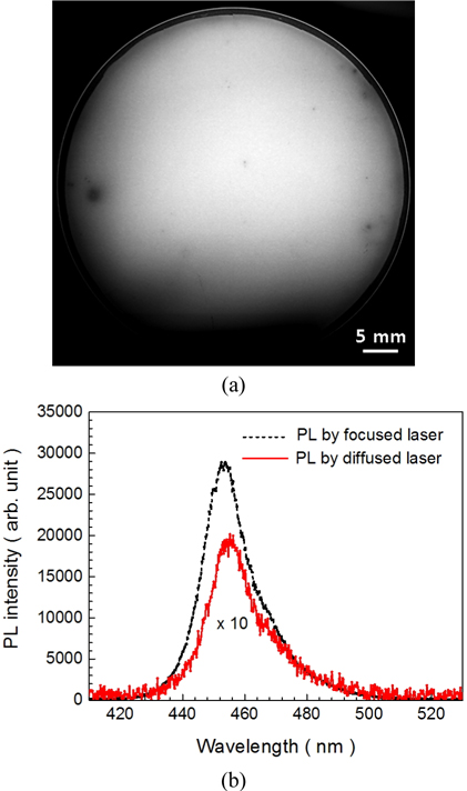
    The images obtained from the PL imaging measurement showed integrated PL intensities for a spectrum range defined by a longpass filter. Figure 2(a) shows a spatial map of the integrated PL intensity of a 2-inch LED epi-wafer obtained using the PL imaging setup. The shape of the PL spectrum obtained under the excitation by a diffused laser beam was not different from that of the spectrum obtained using a focused excitation. There was a difference in the intensity and slight change of the peak wavelength due to the excitation power density difference. Figure 2(b) shows a comparison between PL obtained using a focused excitation and PL under a diffused laser over 2 inch wafer. The integrated PL intensity was displayed in gray scale. In addition, defective regions were observed in the PL images as dark spots of various sizes, as shown in Fig. 2, indicating that PL intensity of the DSDRs was lower than that of other regions.

       3.2. PL Analyses on Defective Regions

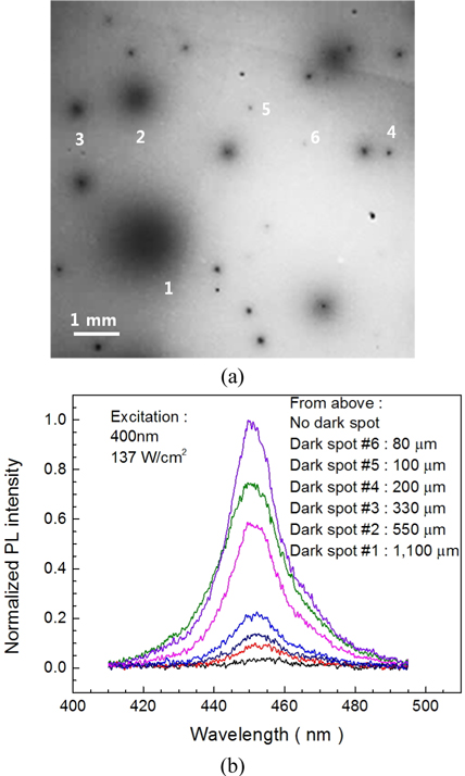
    We measured the PL of DSDRs to analyze their optical properties. Figure 3(a) shows a PL image of a part of a 2-inch LED epi-wafer with DSDRs of various sizes. From the imaged region, dark spots with diameters in the range of ~ 80 μm - 1100 μm were selected, and PL spectra from the centers of the DSDRs were obtained using a 400 nm laser as the excitation source. The laser spot diameter was 50 μm, which was smaller than the diameter of the smallest dark spot considered. Six DSDRs with different sizes and a region with no DSDRs were compared. In Fig. 3(b), the PL spectra of those seven regions under excitation of 137 W/cm2 are shown. The PL intensity decreased as the size of the DSDRs increased, which is fairly consistent with previous reports on microscopic PL intensity imaging [8, 9].

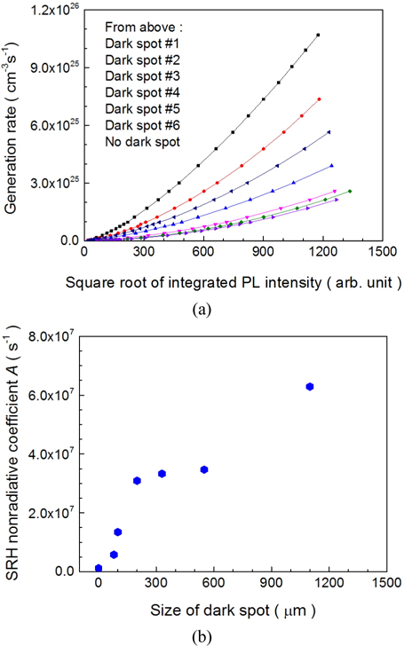
    For the seven regions, the dependence of the integrated PL intensity on the photo-excitation power density was analyzed. The photo-excitation power density (Plaser/Alaser) can be related to the generation rate (G) according to Eq. (1), as described by Dai et al. [12], where Plaser, R, α, Alaser, and are the excitation laser power, reflectivity, absorption coefficient, laser spot size, and laser photon energy, respectively.

    image

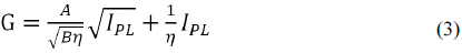
    The generation rate can be expressed using Shockley-Read-Hall (SRH) nonradiative recombination (An) and bimolecular radiative recombination (Bn2) as in Eq. (2) [12]. At the excitation power densities used in this work, the contribution of the Auger process was assumed to be significantly smaller than that of other recombination processes. As the integrated PL intensity (IPL) is proportional to the bimolecular radiative recombination rate (Bn2), Eq. (2) can be modified into Eq. (3), where η is the proportional constant determined by the excited active volumes and collection efficiency of the PL [12].

    image
    image

    Figure 4 shows the relationship between the integrated PL intensity and the generation rate for the seven regions mentioned above. In Fig. 4(a), experimental results (symbols) and fitting results (lines) are shown. The experimental data were fitted using Eq. (3), and we could derive A by assuming that B was 1 × 10⁻¹⁰ cm3/s [12]. The SRH nonradiative recombination coefficient (A) increased with the size of the DSDRs as shown in Fig. 4(b). The nonradiative recombination coefficient of the DSDR with a diameter of 1100 μm was 23 times larger than that of the region with no DSDR. As it has been reported that the SRH nonradiative recombination coefficient (A) is closely related to the dislocation [12] and deep trap densities [13], it could be noted that the DSDRs are aggregations of nonradiative defects mostly originated from dislocations.

       3.3. I-L Characteristics of LED Chips with DSDRs

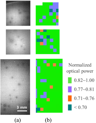
    To investigate the correlation between the PL images and LED chip properties, we fabricated a chip-wafer from an LED epi-wafer whose PL images had been acquired. Photoluminescence images of small areas of the epi-wafer were obtained before starting the LED chip fabrication processes. After the PL imaging, a chip-wafer with LEDs of 1 mm × 1 mm in size with an electrically active area of 0.85 mm2 was fabricated from the epi-wafer. The chip-wafer was evaluated using a chip prober, and the PL imaging results were compared with the chip probing results. In Fig. 5, PL images of small areas of the epi-wafer and optical power mapping obtained from the same areas by a chip prober are shown together for comparison. The optical powers of the chips were normalized, and are shown in different colors according to the normalized power range. The DSDRs in the PL images match well with the chip locations having low optical power. Most of the chips fabricated at the DSDRs showed lower optical powers than the chips at the regions with no dark spots.

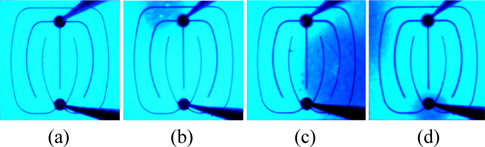
    Individual LED chips with or without DSDRs were further optically and electrically characterized. The properties of the LED chips fabricated at the DSDRs were compared with those of the chips obtained from the regions with no dark spots. When the LED chips were electrically operated, the EL images showed the DSDRs as observed in the PL images. Some of the EL images are shown in Fig. 6.

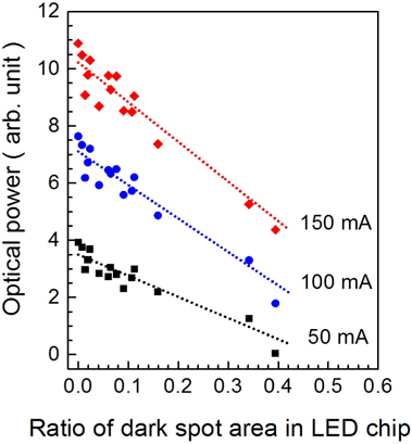
    The I-L characteristics of the chips with DSDRs of various sizes were measured. The optical powers at injection currents of 50 mA, 100 mA, and 150 mA were plotted as functions of the ratio of the DSDR area to the active area of the LED chips as shown in Fig. 7. The optical power decreased with the area ratio of the DSDRs at a given injection current. Choi et al. reported that the dark spot area increased with the dislocation density in microscopic CL mapping images [8]. The area ratio of the DSDRs could be correlated with defect densities in the LED chip, and the increase of the density of nonradiative recombination centers with the DSDR area resulted in the degradation of the optical properties depending on the area ratio of the DSDRs.

       3.4. I-V Characteristics of LED Chips with DSDRs

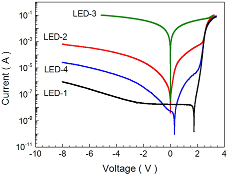
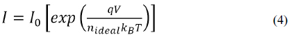
    The I-V characteristics of the LED chips with various DSDR areas were analyzed. Figure 8 shows the semi-logarithmic plots of the I-V curves of the four LED chips shown in Fig. 6. A diode I-V curve above the built-in voltage can be expressed as Eq. (4), where I0, q, kB, and T represent the saturation current, elementary charge, Boltzmann’s constant, and ambient temperature, respectively [14].

    image

    When Eq. (4) was applied to the I-V curve of a chip with no DSDRs (LED-1), the ideality factor, nideal, was 2.8 and 1.7 for bias values ranging from 1.85 to 2.25 V and from 2.3 to 2.5 V, respectively. This result implied that the I-V characteristics were not very different from those of a typical GaN-based LED and there was no significant leakage source in the active layer [15]. However, LED chips with DSDRs in their active regions exhibited different I-V characteristics from LED-1. Huge forward leakages up to the intermediate bias region (~1.2-1.9 V) were observed for the chips with DSDRs. Many researches on leakages of nitride based LEDs reported that the leakages resulted from the defects present in the active regions [16-21]. Several research groups have studied the abnormality of the I-V curve by employing equivalent-circuit models incorporating a parallel resistance and a parasitic diode [14, 21-23]. A low parallel resistance indicates that a significant leakage through routes bypassing the junction exists. The existence of a parallel resistance can be observed near the point of zero current from a linear plot of the I-V characteristics [14]. The leakage source in LED-3 was a parallel resistance, which was calculated from the I-V curve as ~ 50 Ω up to a forward bias of 2.6 V. The I-V curve of LED-2 also showed a linear relationship near the point of zero current, and a parallel resistance of 4 × 10⁵ Ω was critical for the forward leakage at the low bias region. However, as the I-V curve of LED-4 did not show a linear relationship near the point of zero current, the dominant leakage path for LED-4 could not be attributed to parallel resistance.

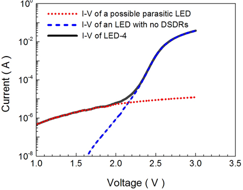
    Tunneling is another important cause of the forward leakage [17-21]. A parasitic diode-like tunnel current at the low-to-intermediate bias deforms the I-V curves from their typical shapes. The I-V curve of LED-4 could be divided into the curves of two parallel diodes as shown in Fig. 9, i.e., the curve of a diode with no DSDRs and little leakage, and that of a possible parasitic diode due to tunneling. The nideal value of the possible parasitic diode was around 18, which was far beyond the nideal value of LED-1. Auf der Maur et al. showed that the nideal value increased up to 14 for LEDs with QWs having thickness larger than the critical layer thickness [18]. Their result suggested that a high dislocation density could be the reason for the high ideality factors. Recently, forward leakage at low and intermediate bias region has been explained considering trap-assisted tunneling [13, 17-19]. The results in this work indicate that the DSDRs in LED-4 are regions of high density of dislocations and deep traps, which cause the forward leakage.

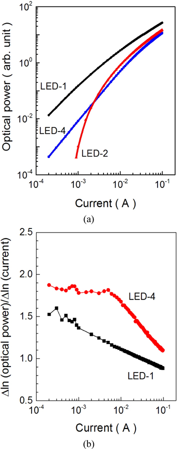
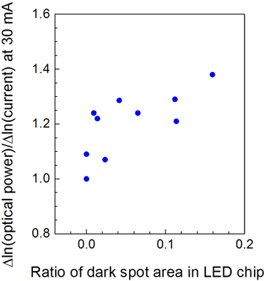
       3.5. Analysis of L-I Characteristics

    The L-I characteristics of LED were fitted with the power law,

    image

    where P is the slope of the logarithmic plot of the L-I characteristic [24-27]. When the radiative recombination process is dominant, P is close to 1, which occurs at high current. On the other hand, when the SRH nonradiative recombination is dominant, P approaches 2, which usually appears at low current. Therefore, the P values can show the influence of nonradiative defects in the active region [24-27]. Figure 10(a) shows the logarithmic plots of the L-I characteristics for LED-1, LED-2, and LED-4. The P values were larger than 5 for the LEDs with small parallel resistances at very low currents, where the influence of the parallel resistance is dominant, as the experimental results for LED-2 show in Fig. 10(a). The P values decreased abruptly as the current increased. The LEDs with little influence of the parallel resistances had P values in the range of ~ 1 - 2 at low currents. Figure 10(b) shows the P values depending on the injection currents of LED with no DSDRs (LED-1) and LED with DSDRs showing tunneling at low current (LED-4). The P value of LED-1 was ~ 1.5 - 1.6 at 2 × 10⁻⁴ A and decreased with the increase of the current. On the other hand, the P value of LED-4 was ~ 1.8 - 1.9 at 2 × 10⁻⁴ A, which was maintained until the current reached 5 × 10⁻³ A, and then decreased. The point where the P value of LED-4 started decreasing corresponded to the current at which the leakage by tunneling on the I-V curve became negligible. The result indicates that the deformation of the I-V curves due to tunneling is mainly related to the SRH nonradiative recombination process. Figure 11 shows the P values of LEDs with various DSDR areas at 30 mA, where the P value of LED-1 was 1 and the effect of the parallel resistance became weak. The P values of LEDs with DSDRs were larger than 1, and showed a weak tendency to increase with the area ratio of the DSDRs, indicating that the influence of the SRH nonradiative process could increase with the DSDRs.

    IV. CONCLUSION

    To inspect GaN-based LED epi-wafers on sapphire substrates, PL imaging based on a vision technology was employed. The PL images showed a spatial map of the integrated PL intensity and DSDRs with degraded luminescence properties over the wide area of an epi-wafer. The DSDRs observed in the PL images were SRH nonradiative recombination centers, and were closely correlated with degraded light intensities of LED chips fabricated from the epi-wafer. The abnormality of the I-V characteristics of the LED chips with the DSDRs resulted from low parallel resistances and/or tunneling due to the defects present in the active regions. The tunneling caused a very high ideality factor (above 18) for the LED with the DSDRs. In the range of the forward bias at which tunneling occurred, SRH nonradiative recombination was the dominant process in the LED operation. The result was consistent with the reports on trap-assisted tunneling, which employed SRH recombination in the models [17-19]. As the DSDRs have a high density of nonradiative recombination defects, which affect the chip operation, the adoption of the PL imaging technique to detect DSDRs can provide an effective inspection and a quick evaluation of LED epi-wafers, allowing the estimation of the properties of the LED chips fabricated from the epi-wafers.

참고문헌
  • 1. Schubert E. F., Kim J. K. (2005) “Solid-state light sources getting smart,” [Science] Vol.308 P.1274-1278 google cross ref
  • 2. Nakamura S., Krames M. R. (2013) “History of gallium-nitride based light-emitting diodes for illumination,” [Proc. IEEE] Vol.101 P.2211-2220 google cross ref
  • 3. Raymond C. J., Li Z. (2013) “Photoluminescence metrology for LED characterization in high volume manufacturing,” [Proc. SPIE] Vol.8681 P.86810 google
  • 4. Aliyu Y. H., Morgan D. V., Thomas H. (1997) “A luminescence mapping technique for rapid evaluation of visible-lightemitting materials used in semiconductor light-emitting diodes,” [Meas. Sci. Technol.] Vol.8 P.437-440 google cross ref
  • 5. Kim H.-T., Kim J., Kim S., Yuh H.-K., Kim D.-H., Ahn D.-H., Shin D.-S. (2013) “A dual side electroluminescence measurement system for LED wafer manufacturing,” [Recent Patents on Signal Proc.] Vol.3 P.49-55 google cross ref
  • 6. Livescu G., Angell M., Filipe J., Knox W. H. (1990) #x201C;A real-time photoluminescence imaging system,” [J. Electron. Mater.] Vol.19 P.937-941 google cross ref
  • 7. Kaneta A., Okamoto K., Kawakami Y., Fujita S., Marutsuki G., Narukawa Y., Mukai T. (2002) “Spatial and temporal luminescence dynamics in an InxGa1-xN single quantum well probed by near-field optical microscopy,” [Appl. Phys. Lett.] Vol.81 P.4353-4355 google cross ref
  • 8. Choi Y.-S., Park J.-H., Kim S.-S., Song H.-J., Lee S.-H., Jung J.-J., Lee B.-T. (2004) “Effects of dislocations on the luminescence of GaN/InGaN multi-quantum-well light-emitting-diode layers,” [Mater. Lett.] Vol.58 P.2614-2617 google cross ref
  • 9. Tamulaitis G., Mickevi?ius J., Dobrovolskas D., Kuok?tis E., Shur M., Shatalov M., Yang J., Gaska R. (2010) “Spatially-resolved photoluminescence study of high indium content InGaN LED structures,” [Phys. Status Solidi C] Vol.7 P.1869-1871 google cross ref
  • 10. Trupke T., Bardos R. A., Schubert M. C., Warta W. (2006) “Photoluminescence imaging of silicon wafers,” [Appl. Phys. Lett.] Vol.89 P.044107 google cross ref
  • 11. Bergman J. P., Jakobsson H., Storasta L., Carlsson F. H. C., Magnusson B., Sridhara S., Pozina G., Lendenmann H., Janzen E. (2002) “Characterization and defects in silicon carbide,” [Mater. Sci. Forum] Vol.389-393 P.9-14 google cross ref
  • 12. Dai Q., Schubert M. F., Kim M. H., Kim J. K., Schubert E. F., Koleske D. D., Crawford M. H., Lee S. R., Fischer A. J., Thaler G., Banas M. A. (2009) “Internal quantum efficiency and nonradiative recombination coefficient of GaInN/GaN multiple quantum wells with different dislocation densities,” [Appl. Phys. Lett.] Vol.94 P.111109 google cross ref
  • 13. Meneghini M., la Grassa M., Vaccari S., Galler B., Zeisel R., Drechsel P., Hahn B., Meneghesso G., Zanoni E. (2014) “Characterization of the deep levels responsible for nonradiative recombination in InGaN/GaN light-emitting diodes,” [Appl. Phys. Lett.] Vol.104 P.113505 google cross ref
  • 14. Schubert E. F. 2006 Light-Emitting Diodes, Chapter 4 google
  • 15. Masui H. (2011) “Diode ideality factor in modern light-emitting diodes,” [Semicond. Sci. Technol.] Vol.26 P.075011 google cross ref
  • 16. Cao X. A., Teetsov J. M., D’Evelyn M. P., Merfeld D. W., Yan C. H. (2004) “Electrical characteristics of InGaN/GaN light-emitting diodes grown on GaN and sapphire substrates,” [Appl. Phys. Lett.] Vol.85 P.7-9 google cross ref
  • 17. Mandurrino M., Verzellesi G., Goano M., Vallone M., Bertazzi F., Ghione G., Meneghini M., Meneghesso G., Zanoni E. (2015) “Physics-based modeling and experimental implications of trap-assisted tunneling in InGaN/GaN light-emitting diodes,” [Phys. Status Solidi A] Vol.212 P.947-953 google cross ref
  • 18. Auf der Maur M., Galler B., Pietzonka I., Strassburg M., Lugauer H., Di Carlo A. (2014) “Trap-assisted tunneling in InGaN/GaN single-quantum-well light-emitting diodes,” [Appl. Phys. Lett.] Vol.105 P.133504 google cross ref
  • 19. Sakowski K., Marcinkowski L., Krukowski S., Grzanka S., Litwin-Staszewska E. (2012) “Simulation of trap-assisted tunneling effect on characteristics of gallium nitride diodes,” [J. Appl. Phys.] Vol.111 P.123115 google cross ref
  • 20. Yan D., Lu H., Chen D., Zhang R., Zheng Y. (2010) “Forward tunneling current in GaN-based blue light-emitting diodes,” [Appl. Phys. Lett.] Vol.96 P.083504 google cross ref
  • 21. Binder M., Galler B., Furitsch M., Off J., Wagner J., Zeisel R., Katz S. (2013) “Investigations on correlation between I-V characteristics and internal quantum efficiency of blue (AlGaIn)N light-emitting diodes,” [Appl. Phys. Lett.] Vol.103 P.221110 google cross ref
  • 22. Masui H., Ive T., Schmidt M. C., Fellows N. N., Sato H., Asamizu H., Nakamura S., Denbaars S. P. (2008) “Equivalent-circuit analysis for the electroluminescence-efficiency problem of InGaN/GaN light-emitting diodes,” [Jpn. J. Appl. Phys.] Vol.47 P.2112-2118 google cross ref
  • 23. Choi I.-G., Han D.-P., Yun J., Kim K. S., Shin D.-S., Shim J.-I. (2013) “Investigation of dominant nonradiative mechanisms as a function of current in InGaN/GaN light-emitting diodes,” [Appl. Phys. Express] Vol.6 P.052105 google cross ref
  • 24. Martil I., Redondo E., Ojeda A. (1997) “Influence of defects on the electrical and optical characteristics of blue light-emitting diodes based on III-V nitrides,” [J. Appl. Phys.] Vol.81 P.2442-2444 google cross ref
  • 25. Cao X. A., Stokes E. B., Sandvik P. M., LeBoeuf S. F., Kretchmer J., Walker D. (2002) “Diffusion and tunneling currents in GaN/InGaN multiple quantum well light-emitting diodes,” [IEEE Electron Device Lett.] Vol.23 P.535-537 google cross ref
  • 26. Meneghini M., Trevisanello L.-R., Meneghesso G., Zanoni E. (2008) “A review on the reliability of GaN-based LEDs,” [IEEE Trans. Device Mater. Reliab.] Vol.8 P.323-331 google cross ref
  • 27. Kim K.-S., Han D.-P., Kim H.-S., Shim J.-I. (2008) “Analysis of dominant carrier recombination mechanisms depending on injection current in InGaN green light emitting diodes,” [Appl. Phys. Lett.] Vol.104 P.091110 google
OAK XML 통계
이미지 / 테이블
  • [ FIG. 1. ]  Schematic of the experimental setup used for photoluminescence (PL) imaging. The equipment in the dashed-line box was used for PL analyses of the selected defective regions.
    Schematic of the experimental setup used for photoluminescence (PL) imaging. The equipment in the dashed-line box was used for PL analyses of the selected defective regions.
  • [ FIG. 2. ]  (a) Photoluminescence image (PL) of a 2 inch blue LED epi-wafer. The excitation power density was 5 mW/cm2. (b) PL spectra obtained by excitation using a diffused laser on 2 inch wafer (red solid line, excitation power density: 5 mW/cm2) and a focused laser beam (black dashed line, excitation power density: 35 W/cm2).
    (a) Photoluminescence image (PL) of a 2 inch blue LED epi-wafer. The excitation power density was 5 mW/cm2. (b) PL spectra obtained by excitation using a diffused laser on 2 inch wafer (red solid line, excitation power density: 5 mW/cm2) and a focused laser beam (black dashed line, excitation power density: 35 W/cm2).
  • [ FIG. 3. ]  (a) Photoluminescence (PL) image of a selected area with dark spot defective regions of various sizes. The excitation power density was 5 mW/cm2. The numbers indicate the defective regions analyzed by excitation power dependent PL. Diameters of the regions: 1, 1100 μm; 2, 550 μm; 3, 330 μm; 4, 200 μm; 5, 100 μm; 6, 80 μm; 7, no defects. (b) Photoluminescence spectra obtained from dark spot defective regions of various sizes
    (a) Photoluminescence (PL) image of a selected area with dark spot defective regions of various sizes. The excitation power density was 5 mW/cm2. The numbers indicate the defective regions analyzed by excitation power dependent PL. Diameters of the regions: 1, 1100 μm; 2, 550 μm; 3, 330 μm; 4, 200 μm; 5, 100 μm; 6, 80 μm; 7, no defects. (b) Photoluminescence spectra obtained from dark spot defective regions of various sizes
  • [ ] 
  • [ ] 
  • [ ] 
  • [ FIG. 4. ]  (a) Relationship between the generation rate from the excitation power density and integrated photoluminescence intensity. (b) Shockley-Reed-Hall nonradiative recombination coefficient as a function of the size of the dark spot defective regions, which was derived by assuming that the radiative recombination coefficient is 1 × 10?10cm3/s for the inspected regions.
    (a) Relationship between the generation rate from the excitation power density and integrated photoluminescence intensity. (b) Shockley-Reed-Hall nonradiative recombination coefficient as a function of the size of the dark spot defective regions, which was derived by assuming that the radiative recombination coefficient is 1 × 10?10cm3/s for the inspected regions.
  • [ FIG. 5. ]  Photoluminescence (PL) imaging results (a) and optical power mapping obtained by chip probing after chip fabrication process (b) for selected areas of an LED wafer. The excitation power density for PL imaging was 50 mW/cm2.
    Photoluminescence (PL) imaging results (a) and optical power mapping obtained by chip probing after chip fabrication process (b) for selected areas of an LED wafer. The excitation power density for PL imaging was 50 mW/cm2.
  • [ FIG. 6. ]  Electroluminescence images of individual LED chips selected from the wafer shown in Fig. 5; (a) LED-1: no defective regions, at 5 mA; (b) LED-2, DSDR area ratio of 0.07, at 10 mA; (c) LED-3, DSDR area ratio of 0.39, at 70 mA; (d) LED-4, DSDR area ratio of 0.16, at 10 mA.
    Electroluminescence images of individual LED chips selected from the wafer shown in Fig. 5; (a) LED-1: no defective regions, at 5 mA; (b) LED-2, DSDR area ratio of 0.07, at 10 mA; (c) LED-3, DSDR area ratio of 0.39, at 70 mA; (d) LED-4, DSDR area ratio of 0.16, at 10 mA.
  • [ FIG. 7. ]  Optical powers of LED chips as functions of the ratio of the dark spot defective region area to the LED active area.
    Optical powers of LED chips as functions of the ratio of the dark spot defective region area to the LED active area.
  • [ FIG. 8. ]  Current-voltage characteristics of selected individual LED chips shown in Fig. 6.
    Current-voltage characteristics of selected individual LED chips shown in Fig. 6.
  • [ ] 
  • [ FIG. 9. ]  Current-voltage characteristic of LED-4 divided into the curves of two parallel diodes: LED with no defective regions and a possible parasitic diode due to tunneling.
    Current-voltage characteristic of LED-4 divided into the curves of two parallel diodes: LED with no defective regions and a possible parasitic diode due to tunneling.
  • [ ] 
  • [ FIG. 10. ]  (a) Logarithmic plots of optical power-current characteristics of different LEDs: LED-1, LED-2, and LED-4. (b) P values for LED-1 and LED-4 as functions of the injection current
    (a) Logarithmic plots of optical power-current characteristics of different LEDs: LED-1, LED-2, and LED-4. (b) P values for LED-1 and LED-4 as functions of the injection current
  • [ FIG. 11. ]  P values of LED chips at 30 mA as functions of the ratio of the dark spot defective region area to the LED active area.
    P values of LED chips at 30 mA as functions of the ratio of the dark spot defective region area to the LED active area.
(우)06579 서울시 서초구 반포대로 201(반포동)
Tel. 02-537-6389 | Fax. 02-590-0571 | 문의 : oak2014@korea.kr
Copyright(c) National Library of Korea. All rights reserved.