Dye-sensitized solar cells (DSSCs) have attracted increasing interest owing to their production cost and high energy conversion efficiency. They are a potential alternative to silicon-based photovoltaic devices [1]. The total photoelectric conversion efficiency of DSSCs has already been enhanced to 13.1% till now [2].
For a DSSC to be functional, dye molecules have to be attached to the TiO2 particle surface. The molecules absorb light, and this excites electrons to higher levels from their ground states. The electrons then pass into the conduction band of TiO2. Thereafter, they percolate through the nanoporous TiO2 structure to a transparent conducting film, flowing through an external load to the counter electrode [2,3].
The extent of conversion efficiency increase has been limited owing to recombination between electrons and either oxidized dye molecules or electron-accepting species in the electrolyte during the charge transport process (2e− + I3− → 3I− ) [4-7]. Recently, this charge recombination has been significantly suppressed by employing thin blocking layers such as those of TiO2, Nb2O5, and ZnO for semiconductors, and CaCO3 and BaCO3 for insulating materials [8-12].
As is already known, SiO2 is a useful material in the microelectronics industry and for thin electroluminescence devices. In researches on electroluminescence devices, it was found that an inserted SiO2 film can remarkably enhance their light extraction efficiency. Sheng et al. [13] exhibited 11.8% enhancement in light output power by inserting a SiO2 current blocking layer (CBL). In addition, Deng et al. [14] increased the efficiency by a factor of two by inserting a SiO2 layer between ITO and the hole-transport layer. However, not many systematic studies have been undertaken to investigate the modification of photoelectric properties by the addition of SiO2 blocking layers.
The overall objective of this research was to evaluate the optical, structural, and photoelectrochemical properties of ITO with different thicknesses of SiO2 used as a buffer and blocking layer in order to obtain high energy conversion efficiency from DSSCs.
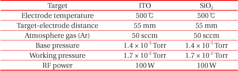
Prior to the experiments, EMP (essential macleod program) was selected to estimate the experimental results. The refractive indexes of all materials were measured using an ellipsometer (UNISEL/M200 with 64CH MWL, HORIBA) to perform an accurate optical simulation. ITO/SiO2 multilayer films were deposited on a soda-lime substrate by DC/RF magnetron sputtering. For the sputtering, high-purity SiO2 ceramic targets (99.99%) and ITO targets (99.99%, In2O3:SnO2 = 90:10 wt%) were used. Sputtering was performed at a substrate temperature of 500℃ in an argon atmosphere with a target-to-substrate distance of 55 mm. The experimental deposition conditions are listed in Table 1. The ITO thickness layer was kept constant at 370 nm. As a blocking layer, SiO2 layers with thicknesses of 0.1, 0.5, 1, and 5 nm were deposited. Additionally, FTO glass with 8 Ω/sq. (Dyesol-Timo) was prepared for property comparison with the ITO electrode used. Transmittance of the multilayer films was measured using a spectrophotometer (Konica Minolta). Further, the sheet resistances of the films were measured using a four-point probe.
[Table 1.] Fabrication of optical thin films by using RF/DC magnetron sputtering method.

Fabrication of optical thin films by using RF/DC magnetron sputtering method.
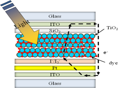
Mesoscopic TiO2 films were prepared via the screen printing method by using TiO2 paste (Solaronix, BN 376c/211013 FM), which is suitable for low-temperature sintering. After screenprinting, the prepared films were sintered under airflow at 150℃ for 30 min. The final thickness of the TiO2 films was approximately 8.9 μm. To adsorb a photosensitized dye on the TiO2 surface, the films were immersed in a Ru complex dye (N719) for 24 h at room temperature. Then, Pt-treated ITO films, which were used as counter electrodes, were placed over the dye-coated films and edges of the cells were sealed with 0.5-mm-wide strips of 60-μm-thick Surlyn (Solarnix, SX 1170, Hot Met). After sealing, an iodide-based electrolyte, tri-iodide in acetonitrile (Solaronix, AN-50), was injected into the cell through two small holes drilled in the counter electrode. The holes were then covered with a small cover glass and sealed. For DSSCs with FTO glass, the experimental methods were the same as those used in the case of DSSCs with the ITO electrode. Fig. 1 shows a schematic view of the interfaces in the DSSCs.
The crystal structure of the films was analyzed by X-ray diffractometry (XRD; Rigaku). The film morphology was observed by field-emission scanning electron microscopy (FE-SEM; JEOL). Atomic force microscopy (AFM) were conducted to study the surface roughness using the model Nanoscope IIIa (Digital Instruments). The photocurrent-voltage (I-V) characteristics of the DSSCs were measured under conditions of AM 1.5 and 100 mW/m2 (1 sun) by using a solar simulator.
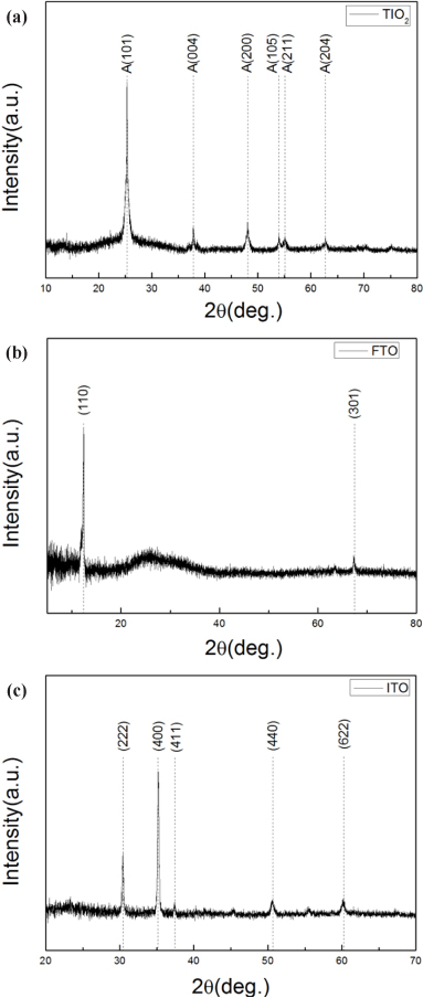
Figure 2 shows the XRD patterns for the ITO, FTO, and TiO2 nanoporous films annealed at 150℃ for 30 min.
The diffraction pattern shown in Fig. 2(a) clearly indicates a tendency for crystallinity in the TiO2 nanoporous film with a (101) preferred orientation at 2 θ = 26.24°.
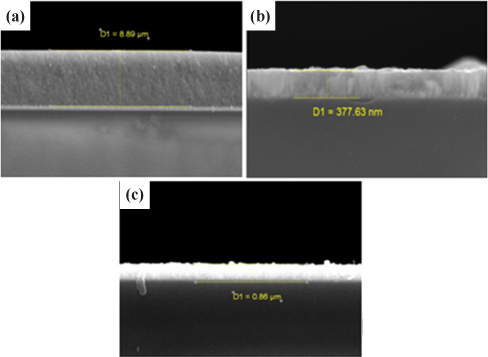
Usually, the anatase phase of TiO2 thin films is formed at temperatures above 250℃ and is then transformed into the rutile phase between 700 and 900℃ [15]. In our XRD experiments, the TiO2 nanoporous films calcined at 150℃ exhibited an anatase phase, even those sintered at a low temperature of 150℃. Thus, the films were crystalline. As shown in Fig. 2(b), the FTO film showed a tendency for crystallinity with a (110) preferred orientation at 2 θ = 12.44°. Further, as can be seen in Fig. 2(c), the ITO film too showed a tendency for crystallinity with (222) and (400) preferred orientations at 2 θ = 30.18° and 35.18°, respectively. Fig. 3 shows the cross-sectional SEM images of ITO, FTO, and TiO2 nanoporous films. From Fig. 3(a), the thickness of the TiO2 nanoporous film was calculated to be approximately 8.9 μm.
The thickness of ITO and FTO films (Figs. 3(b) and (c)) was 377 nm and 860 nm, respectively. In case of the ITO film, the measured film thickness well matched the simulated result (λ1.5 = 370 nm) obtained by EMP.
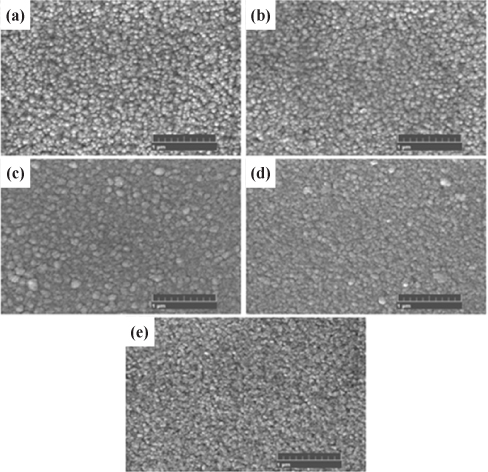
Figure 4 demonstrates the FE-SEM images of (a) bare ITO and ITO films with different thicknesses of the SiO2 thin film: (b) 0.1 nm, (c) 0.5 nm, (d) 1 nm, and (e) 5 nm. The scale bar indicates 1 μm, and grain size was varied from 5 nm to 10 nm. By increasing the SiO2 film thickness from 0.1 nm to 0.5 nm (Figs. 4(b) and (c)), the grain size gradually increased to around 3 nm. However, the grain size continuously decreased thereafter upon further increasing the SiO2 film thickness from 0.5 nm to 5 nm (Figs. 4(c)- (e)).
Since the SiO2 layer was too thin, its thickness could not be confirmed by cross-sectional FE-SEM images and was therefore calculated on the basis of the deposition rate of the SiO2 thin film.
Table 2 lists the summarized results for the refractive index n and extinction coefficient
[Table 2.] Comparison of physical properties of ITO and SiO2 in visible range.
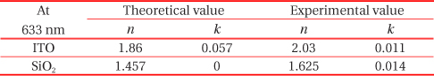
Comparison of physical properties of ITO and SiO2 in visible range.
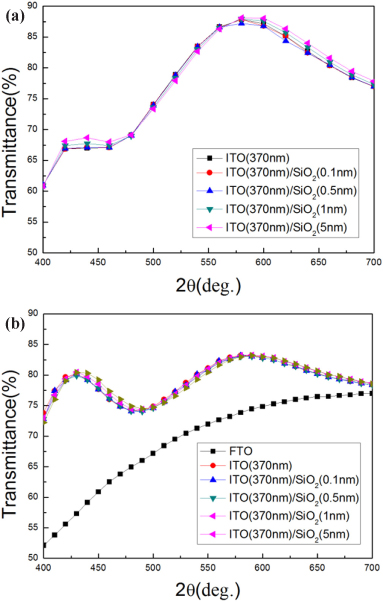
Fig. 5 shows a comparison of the spectral transmittance of various multilayer thin films on the basis of simulated and experimental data.
Figure 5(a) shows the simulation results for the optical transmittance of the ITO/SiO2 multilayer films, calculated using EMP, as a function of the SiO2 thickness. As can be seen in Fig. 5(a), the multilayer films had high transparency in the visible range of 400~700 nm and the transmittance of the ITO/SiO2 thin film slightly increased with increasing thickness of the SiO2 thin film. Fig. 5(b) shows the measured optical transmittance of the ITO/SiO2 multilayer films as a function of the SiO2 thickness. The transmittance of the ITO film was 81% at 550 nm wavelength. Some distinct differences were observed between the experimental and simulated results. The experimentally measured transparency appeared to be somewhat higher than that obtained via simulation for wavelength values below 525 nm. On the other hand, the transparency of obtained from experimental results was lower than that obtained through simulation for wavelength values above 525 nm. This might be attributed to light scattering on the ITO film surface and interface instability due to diffusion. Moreover, the substrate temperature was also considered to cause differences between the experimental and EMP simulation results.
As seen in Fig. 5(b), the transmittance of the FTO film was lower (approximately 10%) than that of all the ITO films. In particular, the transmittance of the ITO film was much higher (up to 23%) than that of the FTO film at wavelengths below 500 nm, where photoelectrodes loaded with the N719 dye absorbed light sufficiently [17] to consume the incident light within the increased light path. Since the ITO film could enhance incident light, short-circuit current (
3.3 Photovoltaic performance of DSSCs
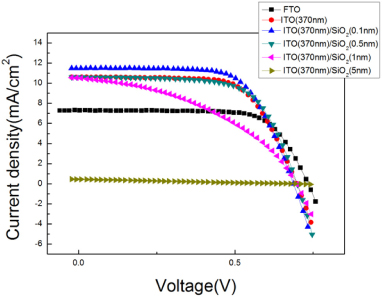
Figure 6 shows the photocurrent density-voltage (
The characteristic parameters for DSSCs can be obtained from the photocurrent density-voltage curve; these parameters are short-circuit current (
The efficiency (

where
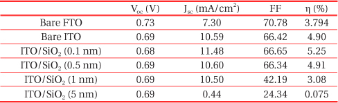
[Table 3.] Comparison of characteristic parameters for DSSCs with thin films.

Comparison of characteristic parameters for DSSCs with thin films.
The DSSC fabricated on the bare ITO film showed a
The DSSC with the 0.1-nm-thick SiO2 deposited ITO film showed the maximum efficiency with 5.259%,
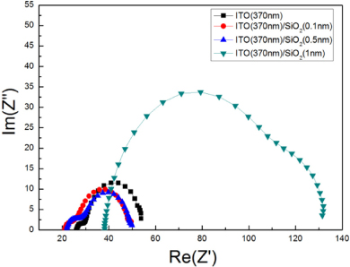
Consequently, the cell performance of DSSCs under illumination seems to indicate a decrease in the recombination rate in the cells, when the 0.1-nm-thick SiO2 film was used as the blocking layer.
Figure 7 shows the Nyquist plots of DSSCs with the bare ITO film, and ITO films with various thicknesses of the SiO2 thin film. As can be seen in the figure, two semicircles were obtained in the Nyquist plots. The larger semicircle in the frequency range 103-10 Hz corresponds to the recombination resistance (
Analysis of the data obtained revealed that the ITO film resistance increased with increasing SiO2 thickness, and this provided supporting evidence for the
In summary, the characteristics of the RF/DC sputtering grown bare ITO film and ITO films with SiO2 blocking layers of various thicknesses were systematically investigated. Compared with the DSSC fabricated on the bare FTO film, the conversion efficiency (
The DSSC based on the ITO film with the 0.1-nm-thick SiO2 blocking layer showed the maximum efficiency with 5.4%. This result is in good agreement with the Nyquist data. Finally, the use of the 0.1-nm-thick SiO2 blocking layer increased the overall efficiency of the DSSC by up to 7.1%.