Metamaterials are artificially constructed sub-wavelength structures, which have increasingly attracted immense attention due to their unprecedented electromagnetic properties such as negative permittivity, negative permeability and negative refractive index media to control light propagation for various purposes [1-4]. A significant breakthrough via metamaterials is to tailor the desired electromagnetic properties and to realize practical devices in the special terahertz region, a band between 0.3 THz to 10 THz that is more rarely explored than radio and optical bands [5-7]. Terahertz devices are designed to control the continuous-wave freely propagating terahertz radiation. The terahertz bandpass filter is one of the most important detection devices, and can be used in Terahertz imaging, spectroscopy, security, biological sensing, and remote sensing applications [8-11]. There is an increasing demand for a terahertz bandpass filter to be designed for higher and wider transmission, thus leading to more practical applications. However, in the terahertz band, most investigators focused on the design and fabrication of narrow filters [12-15] and research on wideband bandpass filters is still limited. The recent trend in THz communication systems is toward frequencies with wide band to obtain even greater increases in communications capacity [16, 17]. This provides an economic incentive to develop THz broadband metamaterial filters.
Recently, Han
In our study, by depositing identical complementary rings on the upper and lower sides of a quartz crystal, a two-layer broadband metamaterial filter was designed and demonstrated. Four samples with different parameters were fabricated using standard microfabrication techniques. Results measured using a THz time-domain spectroscopy system show excellent agreement with those from the simulations. Compared with the broadband filters reported before [18-22], the comple-mentary ring structure in our design is insensitive to any polarization at normal incidence due to symmetry of the ring. Furthermore, the influence of structure parameters (such as period, radius, slot width, thickness and incidence angles) on the transmission has been investigated.
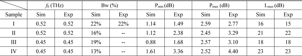
Figure 1 (a) and (b) show the top view and side view of the unit cell for the complementary ring filter, respectively, which consists of three layers, the identical ring slot layers are deposited on the upper and lower sides of a quartz crystal. The transmission frequency response characteristics of the filter can be modeled as an infinite array in CST Microwave software using full Floquet mode implementation to simulate a single unit cell. Periodic boundary conditions are set along the x and y directions with open (add space) boundary in the z direction, then the wave ports are automatically added in the z direction of normal incidence to the structure. During the simulation, aluminum with a conductivity of σ = 3.72 × 10⁷ S/m and thickness of 200 nm is modeled as the metal layer, and the dielectric material is set as crystal quartz with relative permittivity
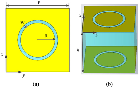
Figure 2 shows the transmission curve (see the solid line) of the complementary ring filter at normal incidence with P = 220 μm, R = 60 μm, w = 10 μm and h = 200 μm. Two resonance poles occur at
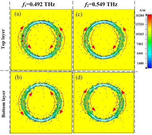
To gain further insight into the resonance modes of the broad transmission, we focused on the electromagnetic response of the ring structure. Figure 3(a) and (b) show surface current distributions at
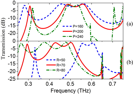
The characteristics of the ring filter actually depend on its geometrical parameters. In the following, parameters with P = 220 μm, R = 60 μm, W= 10 μm and h = 200 μm are considered if it is not otherwise pointed out. Figure 4 shows influence of period P and radius R on the transmittance spectra while the remaining parameters are fixed. In Fig. 4(a), when period P varies from 160 μm to 240 μm, the bandwidth decreases because the relative slot hole becomes smaller in one unit cell and may make little waves transmit through it. At the same time, both the center frequency and the insertion loss of the pass band change little. In Fig. 4(b), as radius R increases from 50 μm to 80 μm, the passband shifts to the lower frequency because the resonance frequency is inversely proportional to the radius [30]. On the other hand, the largest insertion loss in the passband increases with the out-of-band rejection decreasing greatly at the lower frequency. As a result, the passband tends to disappear.
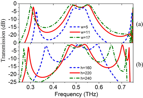
Figure 5 shows the transmittance spectra for various widths w and substrate thicknesses h. In Fig. 5(a), as the slot width increases from 5 μm to 17 μm, both magnitude and bandwidth of the pass band increase because more waves near the resonant frequencies can transmit through this structure, while the out-of-band rejection on both sides tends to decrease. In Fig. 5(b), as the substrate thickness h decreases from 240 μm to 160 μm, the center frequency shifts to the higher frequency.
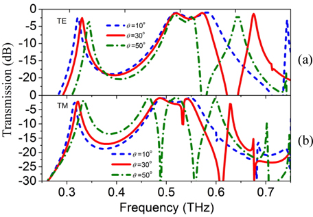
Now, we consider the oblique incident wave, where the electromagnetic waves can be divided into the transverse electric (TE) polarization and the transverse magnetic (TM) polarization. Figure 6 shows the transmission magnitude of the TE and TM polarizations under different incidence angles. For the TE polarization, as angle increases from 0° to 50°, bandwidth of the passband decreases and the out-of-band rejection increases greatly at the higher frequency. For the TM polarization, the broadbands are divided into more narrow bands with angles increasing.
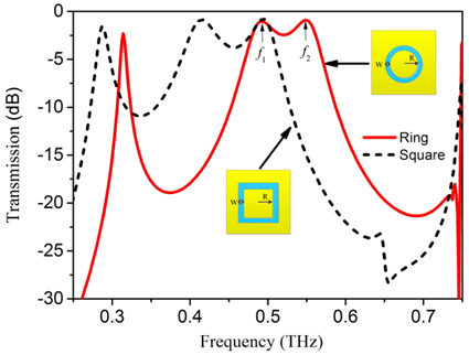
Four samples with different parameters are listed in Table 1. Sample I and sample II have the same parameters with substrate thickness h = 200 μm, radius R = 60 μm, and slot width w = 10 μm, but they have different period P. Sample III and sample IV have the same parameters with substrate thickness h = 230 μm and radius R = 70 μm, but they have different period P and slot width w. Figure 7(a) and (b) show optical micrograph images of sample II at scale 50 μm and 100 μm, respectively. The dark areas are the dielectric layer areas, and the light area is the aluminum coating.
[TABLE 1.] Dimensions of the four fabricated samples (all units in μm)
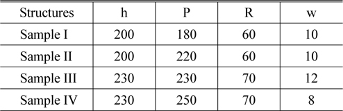
Dimensions of the four fabricated samples (all units in μm)
The samples were fabricated using standard microfabrication techniques and the fabrication process is as follows: the first step was a contact photolithographic process in a photoresist, followed by deposition of a 200 nm Al film on the first side of the quartz substrate by electron beam evaporation. To prevent the metallic patterns from being scratched during the reduction process, a 2000 Å SiO2 film was deposited on the first side of the substrate by plasma-enhanced chemical vapor deposition. Then the substrate reduction process was performed. After the lithography process of the second side of the substrate, the SiO2 film on the first side of the substrate was removed by plasma etching.
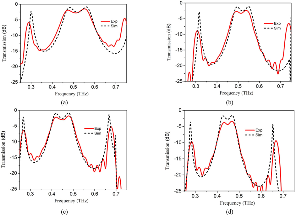
The fabricated samples were measured in THz time-domain spectroscopy [31]. Figure 8 shows transmission curves of the four samples at normal incidence, where the solid and dashed lines denote the measurement and simulation, respectively. It is clearly indicated that broadband bandpass filters have been achieved for the four samples. The measured transmission matches the simulation well except for a slight shift and a larger insertion loss occurred in the measured result. The shift may be caused by dimension error processing. Also, periodic boundary conditions were used to approximate an infinite array in the simulation whereas in the experiment measurements were taken from a finite-sized filter, and hence could have affected shift phenomenon. The larger loss is mainly caused by the finite conductivity of the metal film and the larger dielectric losses in the substrate at the higher frequencies. Using Au as the metallization layer in the simulation, the insertion loss across may be reduced. It should be noted that obvious spurious resonances caused by the etalon (i.e., the Fabry-Perot etalon) occur outside of the passband [32].
To compare the transmission characteristics of the four samples in the measurement with those in the simulation, Table 2 shows the center frequency
[TABLE 2.] Characteristics of the four filters in the simulation and measurement

Characteristics of the four filters in the simulation and measurement
For the simulated result of sample III in Fig. 8(c), the center frequency locates at 0.45 THz with the 3 dB relative bandwidth of 19%. The lowest loss in the passband is 0.88 dB with the dip of 2.57 dB. The largest insertion losses are around 17 dB and 18 dB for the lower and higher frequencies, respectively. In the measurement, the lowest loss in passband is 1.68 dB with the dip of 3.1 dB. For the simulated result of sample IV in Fig. 8(d), the center frequency locates at 0.45 THz with the 3 dB relative bandwidth of 13%. The lowest loss in the passband is 1.61 dB with the dip of 2.52 dB. The largest insertion losses are around 20 dB and 23 dB for the lower and higher frequencies, respectively. In the measurement, the lowest loss in passband is 3.36 dB with the dip of 4.4 dB.
In summary, we have demonstrated the metal-dielectric-metal structure bandpass filters, in which the identical metallic ring slot layers are deposited on the upper and lower sides of the dielectric substrate. The transmission characteristics of the ring and square filters are compared and discussed. It is found that higher center frequency with small insertion loss can be obtained for ring structure with the same parameters. The physical mechanisms of the resonant responses are investigated by surface current distribution. Four samples with different parameters were fabricated and the measured transmissions match the simulations except the slight shift of frequencies and a larger insertion loss in the measurement. The slight shift is mainly caused by dimension error processing. The larger insertion loss may be due to the finite conductivity of the metal film and the larger dielectric losses in the substrate. Finally, influence of the period, radius, width, substrate thickness and incident angles on the transmission is analyzed, respectively. As the period increases, the center frequency changes little while the bandwidth decreases obviously. As radius increases, passband shifts to the lower frequency, both the largest insertion loss in the passband and the out-of-band rejection at the lower frequency decrease greatly. As slot width increases, both the bandwidth and transmission magnitude increase. As the substrate thickness increases, location shifts to the lower frequency with the out-of-band rejections on both sides increase. As incident angle increases, bandwidth decreases for the TE polarization, and the broadband is divided into more narrow bands for the TM polarization.