The past decade has witnessed immense rise in the field of the MEMS. These devices are more preferable as compared to the conventional ones due to miniaturized size. The term RF MEMS refer to the designing and fabricating micro electromechanical system for RF integrated circuits. MEMS switches, working at RF frequencies, are more current than other MEMS devices. MEMS switches are of two types - Series and Shunt. Both types include mechanical movement of a beam that may be due to thermal, piezoelectric, magnetostatic or electrostatic actuation. Because of its small electrode size and virtually zero power consumption, electrostatic actuation is more prevalent.
MEMS switches have been an extensive area of research because they possess low loss, high linearity and high tunable characteristics in comparison with the conventional semiconductor based devices. Many ripened shunt and series designs are previously discussed [1-3] and [4-6]. But the switches are not limited to these two types (series and shunt). A series and shunt switch works between DC - 40 GHz and 10 - 120 GHz, respectively. Many researchers have used the characteristics of these two switches to attain potential results [7,8].
Reliability is the major concern in the field of MEMS switches. Generally mechanical failure is not a major issue because the cantilevers or the fixed-fixed beams are carefully crafted in addition the deflection required for operation of the switch is negligible compared to the length of the beam. Failures in the series switch arise due to the contact metal used while in shunt switches; it happens due to dielectric charging and further, reliability of micro switches in both the cases is affected by the RF power [9]. To increase reliability, the driving voltage for the switch must be low [10]. Driving voltage is dependent on gap, actuation area and stiffness of the membrane. Since isolation will degrade if, the gap is reduced beyond a certain limit, reducing stiffness can cause stiction and self biasing of the beam, so the only option available is alteration in the actuation area.
Research communities have tried to address these reliability concerns and intercalated many approaches like seesaw structures [11], RF disk filter [12] and push-pull mechanism [13]. But the RF performance of these techniques was inferior because they were specifically designed for enhancing reliability. In the present paper, we propose a novel design that focuses on the reliability issues and possesses a superior performance in RF frequencies. As discussed above, dielectric charging and metal contact effect the switch’s lifetime. In the proposed design, metal contact used is hard and has high melting point than the conventional metal and no dielectric have been used. The switch performance is better than [10-13] and operates on a wide frequency band.
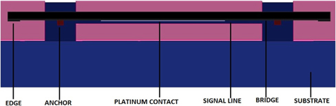
We have used Co-planar waveguide (CPW) which is mounted over the quartz substrate. Modification is introduced in the conventional CPW to achieve better results in RF performance of the switch. The switch consists of 150 μm wide signal line and a gap of 25 μm between the grounds and the signal line on either side. The switch has been optimized at the standard impedance value of 50 ohm.
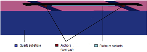
The signal line is split open and length of the open signal line is 100 μm. Over the gap, two anchors of gold are implanted (5 μm × 100 μm × 4 μm) 10 μm apart from signal line on either side. The bridge (300 μm × 100 μm × 1 μm) rests over these two anchors as shown in Fig. 1.
The edges of the bridge are made like cuboids 10 μm in length, 100 μm wide and 2.9 μm in height to increase area and weight at edges. The reason for making the edges thick is to establish the closeness between the bridge and the grounds in the upstate which will maximize the isolation. Moreover, thick edge will increase the weight at corners which would lead to restoration of bridge to up state when actuation voltage is removed thus increasing the anti stiction properties of the switch. The modified bridge with thickened edges is shown in Fig. 2.
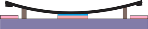
The design is similar to the Raytheon switch design [14]-[16] with some exceptions. Proposed switch is an inline switch designed without use of dielectric and works on the principle of electrostatically actuation by the bias electrode. The proposed switch design is similar to shunt switches and its operation is similar to series switches. The bridge is 3 μm above the signal line and only 2 μm deflection of beam is required for insertion of signal. The reason behind less required deflection is due to implantation of 2 μm thick platinum contact beneath the bridge (shown in Fig. 5) which resulted in reduction of overall movement of the bridge and actuation voltage.
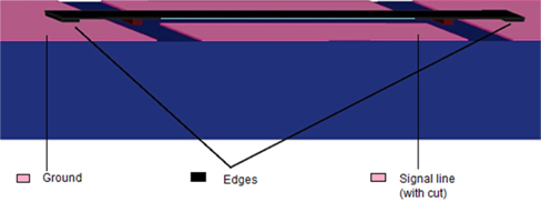
When the bridge is actuated it snaps down and fits into the gap between the signal lines. During operation, bridge is pulled towards the open signal line. Due to bending of bridge, edges get lifted thereby increasing the gap between bridge and ground. Afterwards, the signal is inserted through the signal line because of the continuity of the path introduced due to lowering the position of the bridge. The above described operating principle of the switch is shown in the Fig. 3 and Fig. 4.
The proposed switch is specifically designed to handle the reliability concerns of the MEMS switch and follows a different approach from the former switches. The switch does not use any dielectric material. Moreover, the contact metal used is harder than the conventional metals, this helps in eliminating the problems (i.e. micro welding) that affect switch lifetime. The thickened edges provide additional restoring forces which in turn improves anti-stiction problem of the switch. The switch is designed like a capacitive switch but it operates like a series switch. The switch design is quite simple as compared to former ones to facilitate easy fabrication. The bridge length is much greater than the width and width is much greater than its thickness whereas the deflection of the bridge (2 μm) is much less than the length of the bridge. Hence, mechanical fracture is not a concern for this switch which makes it robust.
The mechanical restoring force on a MEMS beam is given by Equation:

Where F is mechanical restoring force, k is spring constant, g is gap (3 μm), g0 is assumed zero. The preferable range of restoring force is 30 - 120 mN for most switch designs. However, low-voltage low spring-constant beams with k = 1 - 3 N/m result in very low restoring forces and therefore suffer from stiction problems at the metal-dielectric interface (surface tension, contaminants, etc.). The proposed switch exhibits restoring force of 31.2 mN and spring constant of 10.4 N/m, which is above the reliable threshold of 10 N/m [9].
Moreover, the predominant failure in series switches is due to stress on the beam. In the proposed switch, the length of the beam is 300 μm and vertical movement required for the operation is just 3 μm, which is marginal in comparison to the length of the beam. Hence, stress on the beam will be minimal; which makes the switch more durable as compared to conventional ones [16,17].
Bridge - Conventionally in capacitive switches, a uniform bridge is constructed over the two anchors on the ground. This allowed the signal to flow from transmission line to grounds and isolate the output port from the input in down state. But in the proposed design, the bridge is so well designed that it remains very close (0.1 μm apart) to the ground in its upstate and remains remote in the downstate. The bridge is thick at the edges and it provides additional weight. This addition of weight has improved the restoring force of the bridge and helped in removing stiction problem. Any heavy metal (like lead) can be used to achieve this motive.
Note: Bridge could also remain in contact with ground also in upstate. This will further improve the isolation of the switch in upstate but degrade the insertion. So this gap of 0.1 μm helps in achieving the operation as shown in Fig.3.
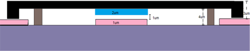
Anchors - Unlike the previous works, anchors are placed in the gap between the signal line and grounds. The design requirements demanded placement of anchors on the substrate (isolation from grounds). Insertion would have degraded to a much higher extent if the anchors were placed on the grounds, but since the anchors are constructed over substrate, signal does not leak from transmission line to the bridge and this promotes insertion and novelty in the design. The cross section of the switch is displayed in Fig. 5.
Contact metal - Gold is commonly used as contact metal but here we used platinum as contact material. The bridge is 100 μm wide, on the edges we have implanted thin layer of platinum metal as shown in Fig. 5. Platinum has a higher melting point and it is harder than conventional contact metal. This will increase the reliability of switch by resisting the welding of the metal at micro level, also known as micro welding.
Substrate serves as the base for the effective fabrication of the switch. The electrical properties and microwave transmission properties of the substrate should be retained even at higher temperatures and over a wide range of frequency. This makes quartz a suitable option for the task. The contact points are made up of platinum. Platinum is harder and it is having high melting point. Use of platinum increases contact resistance but platinum will prevent pitting and hardening which will further restrain stiction. The bridge is made with the use of gold due to its high electrical conductivity. The Table 1 shows various specifications of the switch.
[Table 1.] Switch specifications.
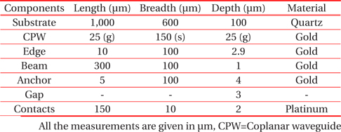
Switch specifications.
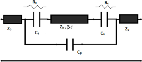
Open ends of the t-line give rise to parasitic capacitance(Cp) and series capacitance(Cs) is between the t-line and the switch metal. Series and parasitic capacitance together constitute Up state capacitance. The total up-state capacitance of the ohmic switch is the same as that of a shunt switch and is given by

But for the switch with two contact points it is given by

Area of t-line (small) and the DC contact area results in the down state resistance of the MEMS switch. Size of the contact area, the mechanical force applied, and the quality of the contact affect the contact resistance. Series switch resistance between the contact areas is dependent on its effective length and width. The total switch resistance for a series switch with two contact area is calculated as:

Where Rs 1 is the signal line loss, Rc is the resistance at contacts and Rl is the resistance of the beam.
The measured insertion loss is - 0.1 dB to - 0.2 dB at 1 - 85 GHz conveying that the switch resistance varies from 1 - 2 ohm.
Measuring S-parameter values or using a circuit simulator we can calculate the loss of a MEMS series switch, as Loss = 1 - |S11|2 - |S21|2. CLR circuit shown in Fig. 6 can also be used for its derivation. The series switch power loss is Ploss = Is2 Rs, where Is is the current in the switch, and Rs is equivalent resistance. Neglecting t-line loss, the ingrain loss of the MEMS series switch is given by:

In the down-state position, Zs = Rs + jwL, and the loss becomes

where Rs is the total resistance of the switch. The loss of the proposed switch is 0.2 dB.
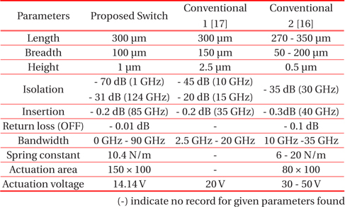
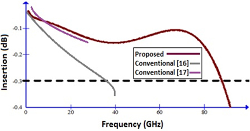
Goldsmith et al. proposed Raytheon switch [16] which is considered as the most mature switch by many because of the number of cycles(i.e. >10 billion cycles) it operated. No other switch performed for such a large number of cycles. Proposed design is similar to this switch in terms of membrane design. Rangra et al. [17] proposed an anti stiction switch and showed excellent performance over a short range of bandwidth. The proposed design comparison is given in the Table with above mentioned two switches.
Table 2, clearly shows that the RF performance of the proposed switch is better than the conventional switches. Required actuation voltage is 0.2 - 0.7 of the conventional switch and bandwidth of the switch is improved 2.7 - 3.5 times over the existing switches.
[Table 2.] Comparison and Contrast between proposed & conventional switches.

Comparison and Contrast between proposed & conventional switches.
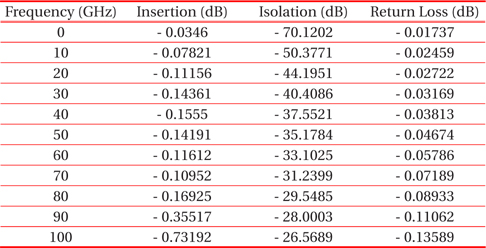
The proposed switch design displays remarkable RF Performance spanning wide bandwidth of 0 GHz - 90 GHz. The switch possesses insertion as low as - 0.03 dB owing to its excellent design. Thus, maximum signal is inserted from input to output port improving the efficiency of transmission. The switch possesses an insertion of - 0.3 dB at 87 GHz. This is well portrayed in Fig. 7.
Isolation of the switch is another milestone in conferring switch as the efficient one. It has been designed such that the switch passes the entire signal to ground in its OFF state. This is achieved with the implementation of anchors over the gap. The switch displays isolation as high as -71.1 dB at 1 GHz and still heading high as - 25 dB at 120 GHz. The switch isolation from 0 GHz - 150 GHz shown in Fig. 8. The isolation of switch deteriorates to - 11dB in a short band from 125 to 127 GHz and after this band the switch again shows isolation loss > - 20 dB.
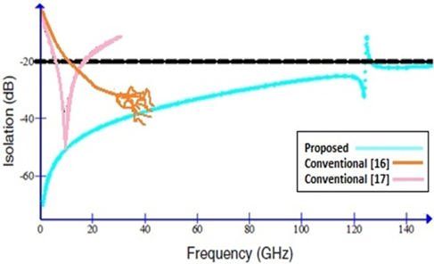
Discontinuity in a transmission line leads to return loss that is the loss of the power in the signal returned. Return loss of the switch in its OFF state is shown in Fig. 9.
The values of insertion, isolation and return loss at various frequencies are tabulated in the Table 3. Thus proposed switch possesses superior RF performance and is operable over wide bandwidth.
[Table 3.] Values of RF Parameter.

Values of RF Parameter.
Spring Constant plays an important role in mechanical operation of the beam. It can be approximated by assuming that actuated electron does not bend. The spring constant for the above designed beam is given as
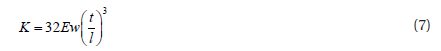
Where E is young’s modulus of silicon, l is length of the beam, w is the breadth and t is the thickness of the beam.
Analytically, the spring constant for the proposed beam is 10.42 N/m.
The ‘pull-down’ voltage required to pull the bridge over the signal line thus facilitating conduction is known as actuation Voltage. The actuation voltage is supposed to be kept as low as possible for flexible operation. Applying actuation voltage helps in developing the electric field directed vertically downward that exerts force on the beam. The increased force pulls the beam downward which results in decreasing beam height and increasing capacitance.
The actuation voltage is given by Vp.
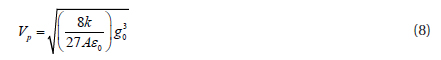
where k is the spring constant, 0 is the permittivity of free space, A is given by the area of actuation and g0 is the gap between cantilever and signal line. Actuation Voltage of the proposed switch is found to be 14.14 V which is much less than 20 V and 30 V required in [17] and [16]; thus making the switch suitable for Low power applications (Satellite Communications) where the power conservation is the prime concern.
Restoring Force is the force required to restore the beam to its equilibrium position as and when the actuation voltage is removed. It is given by

Where K is the spring constant of the beam and x is the gap between signal line and beam. The restoring force of the beam for the proposed design is found to be 20.8 μN.
The proposed switch displays novelty in its design considerations and exercise remarkable RF Response in wide Frequency band. The switch is operable from DC to 90 GHz. Switch has been designed considering the stiction problem and reliability issues. Bridge has been designed such that additional weight at the two longitudinal edges prevents stiction, once the actuation voltage is withdrawn. The bridge possesses high restoring force which aids in maintaining equilibrium i.e. reviving the bridge into its up state. The switch possesses an insertion loss as low as - 0.03 dB at 1 GHz that rises till - 0.3 dB at 90 GHz. High Isolation loss provides the switch with an extra point as switch works with isolation as high as -31 dB to the frequency of 124 GHz. Required actuation voltage for the switch operation is 14.41 V which is much less than formerly designed switches. The switch would find extensive application in wideband operations and areas where reliability is a major concern.