ZnO based thin film transistors (TFTs) | have advantages of high mobility and low temperature in device fabrication. They were regarded as transparent TFTs (TTFTs) since they also have high transparency in a visible range [1-3], Amorphous InGaZnO (a-IGZO) was regarded as a channel layer of TTFT due its good performance, transparency, and stability [4]. There are many studies of channel layer as well as source and drain (S/D) electrodes of TTFTs, because the S/D electrodes have an effect on the electrical performance and transparency of TTFTs. Transparent conductive oxides (TCOs) were suited for the S/D electrodes of TTFTs due to a high optical bandgap (> 3.5 eV), good electrical conductivity, and high optical transparency, 80% in visible-infrared. Particularly, amorphous indium zinc oxide (a-IZO) was used for an S/D electrode of ZnO TTFTs due to its high transparency and lower resistivity. Although there was a lot of research regarding S/D electrodes of ZnO based TFTs, such as the transparency, resistivity, and contact problem with the channel layer, the relation between the stability of ZnO based TFTs under the various stress and S/D electrodes is still unknown [5-8].
Proposed in this letter is the influence of S/D electrodes on the stability of a-IGZO TFTs. The change of S/D electrodes had an effect on interfacial traps and energy barriers between channel layers and S/D electrodes. The different behavior of electrical performances of a-IGZO TFTs has been studied depending on the S/D electrode.
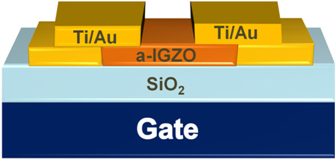
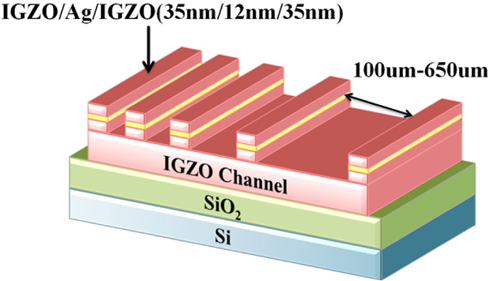
The a-IGZO TFTs were fabricated with the use of a thermally grown SiO2 thin film on a highly p-type Si (001) substrate as both substrate and gate electrode. The a-IGZO layer (50 nm) was deposited using an rf magnetron sputtering with channel width (250 μm) and the channel length (Lch) ranged from 100 μm to 650 μm. All devices were annealed at 350℃ for 1 h in N2 ambient; the different electrode was deposited and patterned using the lift-off method. The Ti (10 nm) and Au (60 nm) as S/D electrodes were deposited by an e-beam and thermal evaporation, respectively, as shown in Fig. 1. The a-IZO electrodes and a-IGZO layer of a-IGZO/Ag/a-IGZO electrodes were grown by an rf magnetron sputter method and the Ag was deposited using the thermal evaporation. Transfer characteristics are measured at a drain voltage VDS of 5.1 V with a single-sweep gate voltage VGS mode from -20 to 40 V. The Vth is defined as the VGS value where a drain current IDS of 5 nA flows.
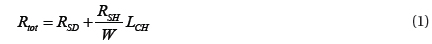
In order to investigate specific contact resistance with various electrodes, the transfer line method (TLM) was used, as shown in Fig. 2, with an OMO electrode. Total resistance (Rtot) was determined from the slope of the linear region of the output characteristics. Rtot is a function of the contact resistances (RSD) of the two contacts and the sheet resistance (RSH) of the semiconducting layer outside the contact and RSD and RSH were obtained from the y-axis intercept and slope the Rtot - LCH plot of Figure 2, respectively, by Equation (1) [9,10]:

where LCH is the separation of the electrodes, and W is the electrode width fixed at 250 μm. The RSD with Ti /Au was higher than that with the a-IZO and IGZO/Ag/IGZO electrodes and the ratio of RSD /RSH was also higher as reported before [13]. This is mainly due to a low energy barrier between the channel and S/D electrodes, so the oxide electrodes made it easier to inject the carriers into the channel layer. Therefore, the IGZO/Ag/IGZO electrodes were best for S/D electrodes of a-IGZO TFTs from the aspect of contact resistance.
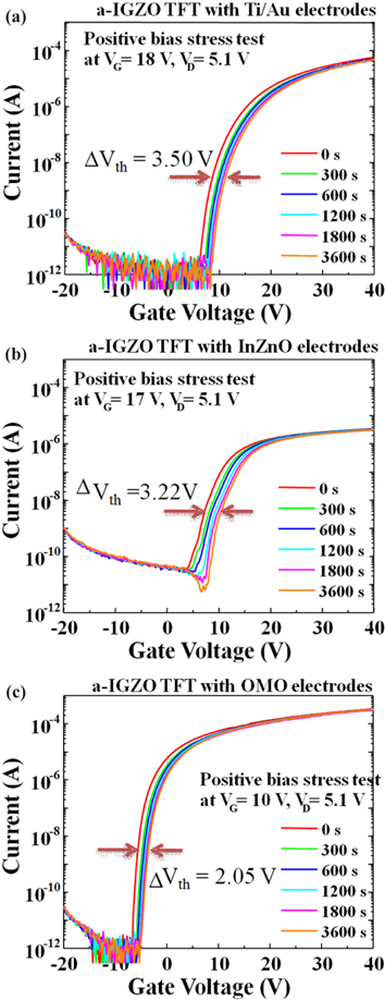
Figure 3 shows the positive bias test of all TFTs under the following conditions: the VDS and IDS were fixed at 5.1 V and 10 μA, respectively and VGS of 18, 17, and 10 V was applied for Ti/Au, a-IZO and OMO electrodes, respectively. The maximum stress duration was 3,600 s. The positive Vth shift (ΔVth) of a-IGZO TFTs has been explained by two mechanisms: charge trapping or defect creation. In the case of charge trapping, the parallel shift in Vth without a significant change in the S value is attributed to a simple charge trapping in the gate dielectric and/or at the channel/dielectric interface. On the other hand, the ΔVth caused by the creation of defects in channel materials accompanied the change in S comes [11,12]. ΔVth of the positive bias test was reduced with OMO electrodes. However, all devices with top S/D electrodes had the same trap density in bulk and interface between channel and gate insulator since all the process parameters were fixed before the deposition of the S/D electrode. Therefore, it is clear that the trap density was changed depending on the S/D electrodes or contact of S/D electrodes with a-IGZO channel layer.
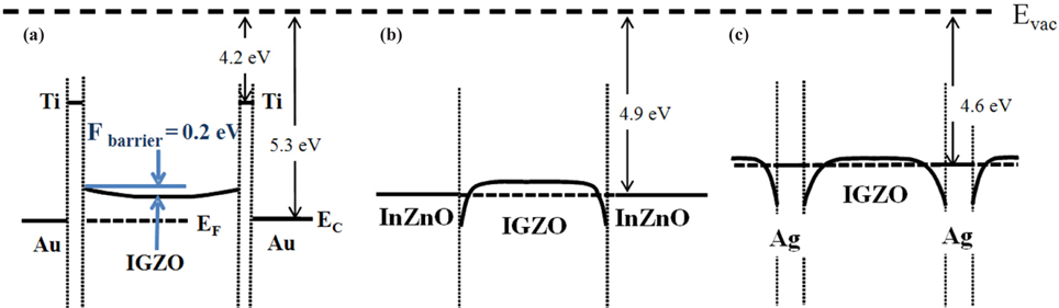
Based on these results, we built a band diagram of a-IGZO TFT depending on the S/D electrodes as illustrated in Fig. 4. It was known that the work function of the a-IGZO, Ti, Au, IZO and Ag was 5.1, 4.3, 5.3, 4.9, and 4.6 eV, respectively [14,15]. As illustrated in Fig. 4 (a), (b), and (c), the contact between a-IGZO and Ti/ Au electrodes had a Schottky barrier while the contact of the IZO and IGZO/Ag/IGZO electrodes with channel layer was an ohmic contact. Figure 4(d) and (e) shows the band diagram of TFTs with Ti/Au and IZO electrodes when the positive bias was applied. The electrons in a-IGZO TFT with Ti/Au electrodes was trapped in trap states at the Schottky barrier of drain electrodes. In the cases of IZO and OMO electrodes, trapped electrons were hardly observed in drain electrodes due to the ohmic contact. It is interesting to note that the a-IGZO TFT with a-IZO electrodes show the aging effects during the stress test while OMO does not. These results indicate that an OMO electrode is suitable for an a-IGZO TFT with all respects, such as electrical performance, contact resistance, and stability.
In conclusion, the effect of S/D electrodes of the a-IGZO TFTs has been investigated. The electrical properties and stability of an a-IGZO TFT shows the different trend with S/D electrodes. The a-IGZO TFTs with an a-IGZO/Ag/a-IGZO of S/D electrodes had good performance and low contact resistance due to the homo-junction with channel layer. In addition, significantly improved stability of positive bias was obtained at the a-IGZO TFTs with a-IGZO/Ag/a-IGZO electrodes. Therefore, both specific contact resistance and stability of a-IGZO TFTs were improved with multilayered electrodes of IGZO/Ag/IGZO.