Zink based oxide semiconductor has been attracting attention due to its potential application in transparent displays, solar cell, transparent electronic skins and transparent electrodes [1-3]. ZnO instead of ITO (Indium Tin Oxide) has usually been used with impurity doping, such as Al, In, Ga, Cu or Sn for high conductivity, and it is known that the electrical properties of Zink based oxide semiconductors usually improves with the annealing processes. The current of oxide semiconductors originates from the conductivity, due to the donor, such as Zn ions (Zni2+) or oxygen vacancy ions (Vo2+). ZTO is made by the mixing of ZnO:SnO2, 1:1, and there are ZnO of n-type and SnO2 of p-type. ZTO without an indium has a merit low production cost. Zink based oxide semiconductors with high mobility must decrease the resistivity and mismatching at the interface between a channel and dielectric material [4-9]. Also, the understanding that a contact mechanism at the interface in a device is also an important factor. The Schottky and Ohmic contacts for semiconductors depend on the Schottky barrier, and the Ohmic contact has no potential barrier, so the current-voltage curves has linear properties. The Schottky barrier has a potential barrier and has a non-linear I-V curve, because of the depletion layer, which is due to the electron-hole combination [10-12]. There are many studies concerning the oxygen vacancy and structure, but the correlation between oxygen vacancy [13-15], structure and electronic properties remain un-researched.
In this study, it was demonstrated the effects of oxygen vacancy and electronic properties by using the ZnO, SnO2 and ZTO. To understand the electrical properties of ZTO, ZnO, SnO2 and ZTO, they were prepared with an oxygen gas flow rate of 20 sccm on p-type Si wafers. As-deposited films annealed at 100℃ and 200℃ to generate the difference in depletion layer in accordance with the ionization state. All samples were analyzed in terms of the PL, XRD, XPS and contact properties observed from the I-C curves. The correlation between the oxygen vacancy and bonding structures with increasing the annealing temperatures was induced.
ZnO, SnO2 and ZTO were deposited with oxygen gas flow rates of 20 sccm on p-type Si substrates at room temperature using RF magnetron sputtering for 10 minutes [16]. As-deposited samples were annealed at 100℃ and 200℃ in an air condition to observe the temperature dependency of ionic diffusion currents and conductions by the oxygen vacancy.
The ZnO SnO2 and ZTO targets (99.99% purity) were supplied by ANP Co., LTD. Al source/drain electrodes were evaporated by a thermal evaporator. The current-voltage were measured using MIS (metal/SiOC film/Si) structure and mask pattern with a diameter of 200 ㎛. Aluminum was used as the electrode source. Electrical characteristics of current vs voltage were measured using the semiconductor parameter analyzer (4155A). Measurements were carried out in dark conditions, in air. All samples were analyzed in terms of the PL, XRD and XPS.
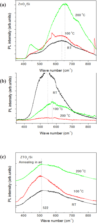
Figure 1 shows the PL spectra used to research the optical properties of the oxide semiconductors of ZnO, SnO2 and ZTO. The wave length of ZnO was observed as the longest, and that of SnO2 was the second longest, and that of ZTO was the shortest. As such, it could be forecast that the energy gap of ZTO is the highest, and that its electrical properties can be improved more than ZnO and SnO2. The ZnO, SnO2 and ZTO films were deposited and then annealed at 100℃ and 200℃, to research the correlation between oxygen vacancy and the electrical properties.
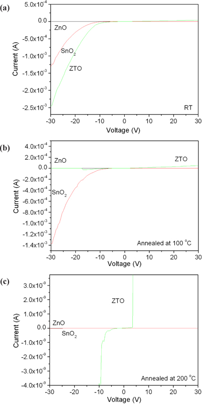
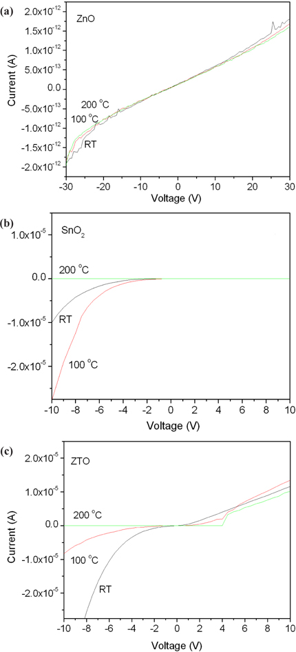
Figure 2 shows the electrical properties of ZnO, SnO2 and ZTO with a structure of Al/semiconductor/p-Si. A ZnO film demonstrated the Ohmic contact depending on the voltages in accordance with the annealing temperatures. However, that of SnO2 and ZTO are nonlinear Schottky contacts. Moreover, the current decreases with increased annealing temperatures because the oxygen vacancy as an ionic state decreased during the annealing processes. In spite of this, the annealing effect of the oxygen vacancy did not affect the ZnO film, which has Ohmic contact despite annealing. The Ohmic contact is due to the impurity doping carriers, and the oxygen vacancy (Vo2+) as an ionic state is weakly related to the Ohmic contact [17,18]. To observe the relationship between the oxygen vacancy and crystallization during the annealing processes, all samples were analyzed for their XRD patterns.
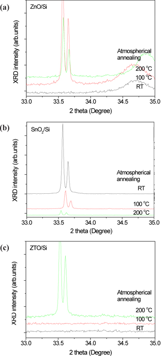
Figure 3 shows the crystallization properties of ZnO, SnO2 and ZTO. Oxygen semiconductors commonly show the peaks at 33.5 degrees. A ZnO has 33.5 and 34.7 degrees with a broadened peak. A SnO2 film decreased the crystallization with increased annealing temperatures, in spite of ZTO of high crystallization with increased annealing temperatures. The crystallization of ZnO and ZTO increased at high annealing temperatures, because of their high density structure due to arrangement between the doping carriers. However, the structure of an annealed SnO2 becomes amorphous because of a depletion layer due to the electron-hole combination from the oxygen vacancy and metal oxygen prepared after deposition. The increase in the depletion layer causes the Schottky contact and limits the current as is shown in Fig. 2.
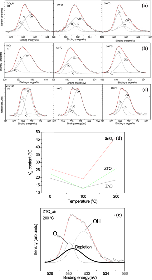
Usually, it is known that the conductivity of an oxide semiconductor depends on its oxygen vacancy. One atom of oxygen becomes two electrons, after the ionization by annealing or deposition. The oxygen vacancy (Vo2+) as the donor ions can contribute a conductance after the extraction of electrons. As such, the oxide semiconductor after the annealing increases the density of oxygen vacancies and improves the electrical properties. However, the oxygen vacancy fills with oxygen from the air during the annealing and then decreases the conductivity, as is shown in Fig. 2. It was confirmed that the ZnO with annealing processes is not related to the formation of oxygen vacancy from the results of Fig. 2 and Fig. 3. The oxygen vacancy is generally defined by the analysis of O 1s spectra, using the XPS.
Figure 4 outlines the deconvoluted O 1s spectra of all samples. There are the first Om (metal oxygen), the second oxygen vacancy (Vo2+) and the third OH peaks, each with the highest binding energy [19,20].
Figure 4(a) and (b) shows how the OH bonding decreased with an increase in annealing temperatures. Figure 4(c) displays the main peak, with a shift to low binding energy in accordance with the increase in annealing temperatures. Figure 4(d) shows the relative content (%) of oxygen vacancy (Vo2+) obtained from the O 1s spectra. The oxygen vacancy of ZnO did not increase with increments of annealing temperatures. The oxygen vacancy of ZnO annealed at 100℃ steeply decreased, and that of ZnO annealed at 200℃ in compared with as-deposited ZnO (RT) film was also low content. However, the oxygen vacancy of SnO2 annealed at 100℃ decreased, and that annealed at 200℃ steeply increased. These results indicate that the properties of ZTO observed from oxygen vacancy follow the characteristics of SnO2. The oxygen vacancy of ZTO annealed at 100℃ decreased, and that annealed at 200℃ steeply increased. As seen in Figs. 2 and 4, the oxygen vacancy was related to the electrical properties, which was affected by the amorphous structure. However, the oxygen vacancy was not related to the crystal structure. Moreover, the oxygen vacancy of ZnO with a high crystal structure decreases with increasing the annealing temperature. The electrical properties of ZnO did not change with increasing the temperature as shown in Fig. 2(a). Therefore, it is natural that the oxygen vacancy is related to the depletion region as shown in Fig. 4(e).


OH groups formed during a deposition were evaporated during the annealing process and the recombination between metal oxygen and the oxygen vacancy became a depletion region. ZnO had an Ohmic contact and a structure of crystallization with increased annealing temperature because of the absence of ionic charges and a depletion region. SnO2 involves a Schottky contact because of the depletion region due to the combination of ionic groups, such as oxygen vacancy and metal ions with increased annealing temperature. The formation of a depletion region in the semiconductors is an important condition to become a Schottky contact.
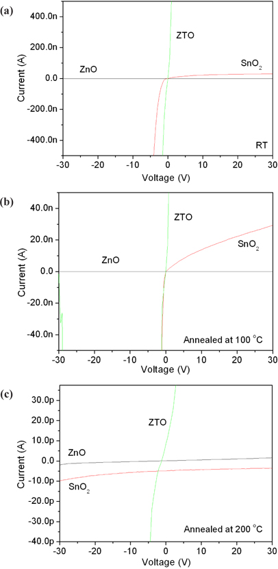
Figure 5 shows the current-voltage characteristics depending on the annealing temperature to study the contact properties of ZnO, SnO2 and ZTO, as shown in Fig. 2. Figure 5(a) shows the I-V curves of ZnO with non-conductivity compared with SnO2 and ZTO with Schottky contacts. Figure 5(b) is the I-V curves of SnO2 annealed at 100℃ with good conductivity. Figure 5(c) shows the I-V curves of ZTO annealed at 200℃ with an ambipolar Schottky contact.
To compare the relative electrical properties of ZnO, SnO2 and ZTO, Fig. 6 shows the temperature dependence of the electrical characteristics of ZnO, SnO2 and ZTO in a range of
The oxide semiconductors, ZnO, SnO2 and ZTO were annealed at various temperatures were analyzed by XPS, XRD and I-V curves to research the correlation between their electrical properties and structures. ZnO had an Ohmic contact and crystal structure. However, SnO2 and ZTO showed Schottky contact with increments of increased annealing temperatures. The effect of oxygen vacancy was not proportionate to the electrical properties of oxide semiconductors. Oxygen vacancy was closely related to Schottky contact and weakly related to the Ohmic contact. The annealing progress was enhanced upon the combination of oxygen vacancy and metal oxygen, and made the depletion region a Schottky contact. The electrical properties of ZTO with a Schottky contact, due to the SnO2, became stable and had improved performance with increased annealing temperature.