The development of science in the 20th century has contributed greatly to human civilization, especially, in the evolution of displays and the internet. In addition, the 21st century has come with great capacity and the information age based on high-speed information processing technologies. The basis of information processing technology is the various developments of large and small displays according to the contributions of computers and telecommunication. Recently, light-emitting diode (LED) has been applied to a display. The LED is classified as inorganic and organic LED. For the inorganic LED, the driving voltage of the device is 100 [V] or more, and it is difficult to fabricate large displays because the device is produced by vacuum deposition [1]. In particular, a blue LED is difficult and expensive. However, the OLED has a great advantage for display because it can overcome the disadvantage of inorganic LED [2,3]. Thus, the OLED is a promising device in the future, because it can easily produce various colors depending on the choice of synthesized materials. Conventional displays such as CRT, PDP, and TFT-LCD are expected to be replaced by the flexible OLED [4].
In 1963, Pope et al., studied LED made with organic material composed of anthracene mono-crystalline [5,6]. The device using the anthracene was composed of a thick crystal and required a high driving voltage of around 100 [V]. The power conversion efficiency of the device using the anthracene was ≤ 0.1%, and the external-quantum efficiency was at least 5%. In 1987, Tang and VanSlyke reported green OLED operated at a low voltage by using a low molecule [7,8]; and subsequently in 1990, Friend in Cambridge University reported green OLED using the polymer PPV. Since then, tremendous research has been carried out to obtain the OLED with high efficiency and robust durability [9,10]. Several studies were conducted in order to understand conduction mechanism and dynamic behavior of charge carriers. The necessity of research on the equivalent circuit analysis led to studies, such as that of Roy, who analyzed the equivalent circuit including the organic layer to a resistive component and a capacitive component [11,12]. Pospisil reported that complex impedance is affected from the resistive to the capacitive contribution depending on the frequency and the applied voltage [13]. In 2013, Narayan et al., studied an effect of hole injection and hole blocking layer on the performance of OLEDs with the use of CuPc and bathocuproine (BCP), respectively [14]. In this paper, we present the influence and effect on the electrical properties of the OLEDs with an insertion of electron-transport layer of BCP.
Indium-Tin-Oxide (ITO) substrate was used as an anode, which has a surface resistance of approximately 8 [Ω/sq].
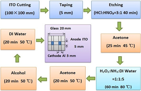
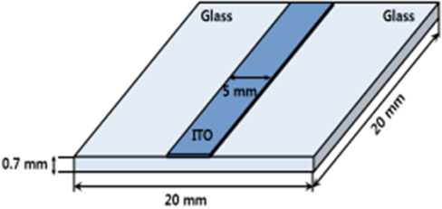
Figure 1 shows the patterned shape of the ITO electrode. The size of the glass is 20 [mm] × 20 [mm] and that of the patterned ITO line is 5 [mm] × 20 [mm].
Figure 2 shows the process involved in making the ITO anode. At first, insulating tape is attached on top of the ITO glass with a width of 5 [mm]. The place that is not taped on the ITO glass, was etched by exposing it to the stream of aqua regia mixed with hydrochloric acid (HCI) and nitric acid (HNO3) with a volume ratio of 3:1 for 40 [min]. Ultrasonic wash was conducted in acetone for 25 [min], subsequently, in the solution mixed with ammonia and hydrogen peroxide and deionized water of volume ratio 1:1:5 at 80℃ for 60 [min]; and again, in acetone at 50℃ for 20 [min]; and finally in isopropyl alcohol at 50℃ for 20 [min]. After the ultrasonic cleaning, deionized water was applied for 20 [min] and it was completely dried.
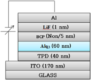
Figure 3 shows a device structure of the OLED in our experiment; ITO(170 nm)/TPD(40 nm)/Alq3(60 nm)/BCP(0 or 5 nm)/LiF(1 nm)/Al. ITO and Al are used as the anode and cathode, respectively. The BCP layer is made to 0 or 5 nm thickness. For the deposition method, all the organics are deposited using thermal vapor deposition at a pressure of 5 × 10⁻⁶ [Torr]. Deposition rates of TPD, Alq3, and (BCP and LiF) are 1.0 [Å/s], 1.5 [Å/s], and 0.2 ~ 0.3 [Å/s], respectively. Al of 99.99% purity purchased from Aldrich Co. is evaporated using a tungsten boat. The active area of the device is made to a size of 3 × 5 [mm2] by using a shadow mask.
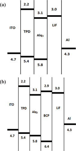
Figure 4 shows the energy-level diagrams of the OLEDs (a) with and (b) without the BCP layer. The values of HOMO (Highest Occupied Molecular Orbital) and LUMO (Lowest Unoccupied Molecular Orbital) for the hole-transporting TPD material are 5.4 [eV] and 2.2 [eV], respectively; those for the emissive Alq3 material are 5.8 [eV] and 3.1 [eV], respectively; those for the electron-transport BCP material are 6.4 [eV] and 2.9 [eV], respectively; and LUMO of the electron-injecting LiF material is 3.0 [eV].
The value of LUMO is decreased by approximately 0.6 [eV[ with insertion of the electron-transport BCP layer. The injection of the electron is facilitated due to decreases in the value of HOMO by approximately 0.6 [eV],. The device performance is improved by the increases in recombination rate of the electron and the hole due to blocking of the hole transport [15]. Four organic materials are used in our device fabrication.
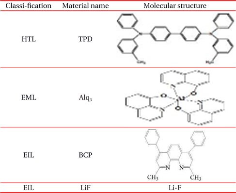
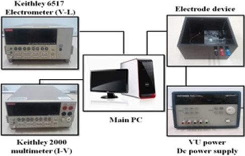
Table 1 shows the name and the molecular structure of the organic materials used. In this experiment, the current density-voltage-luminance characteristics of OLEDs are measured with the Keithley 6517 electrometer and Keithley 2000 multimeter, and a Programmable Vupower Co. as the DC Power supply. Lab-view program is used to control the voltage and the current, and the silicon photodetector is placed at the front of the device to measure the photocurrent. The DC current is measured with the Keithley 2000 multimeters depending on the applied voltage.
[Table 1.] Name and molecular structure of the organic materials.

Name and molecular structure of the organic materials.
Figure 5 shows the schematic of the current density-voltage-luminance measuring system.The photocurrent is proportional to the number of photons generated by the illumination of light to the photodector, and the DC current flowing through the device is proportional to the number of electrons. Therefore, the light-emitting efficiency and the external-quantum efficiency of the device are obtained through the photocurrent and the DC current. All the experiments are conducted at room temperature; the applied voltage to the device is increased by 0.25 [V/s]; and the measuring delay time is 1,000 [ms].
3. EXPERIMENTAL RESULTS AND DISCUSSION
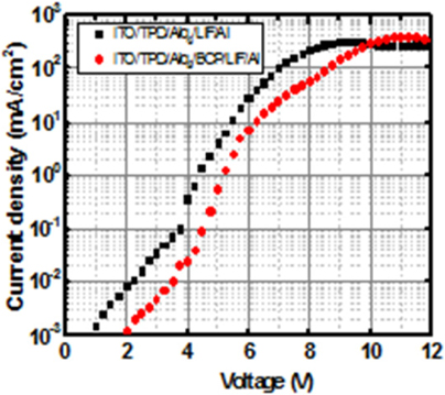
Figures 6 shows the current density-voltage characteristics for the devices with/without the electron- transport BCP layer. Even though the figure shows a similar nonlinear characteristic, there is a difference in current density below 10 [V] for the devices with/without the BCP layer. However, when the applied voltage is above 10 [V], the current density in the device with the BCP layer is slightly higher than that without BCP layer.
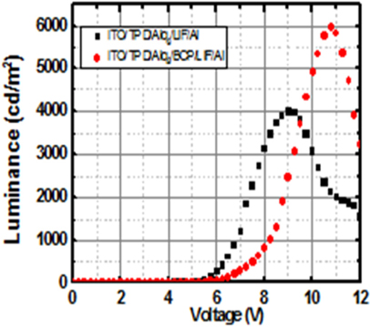
Figure 7 shows the corresponding luminance-voltage characteristics of the devices. The luminance characteristics become distinct above 6 [V]. Use of BCP layer to the device results in improvements of maximum current density and maximum luminance by approximately 22[%] and 50[%], respectively. The maximum current density is 305.6 [mA/cm2] and 373.4 [mA/cm2], and the maximum luminance is 4,004 [cd/m2] and 5,989[cd/m2] for the devices with/without the BCP layer, respectively. It is thought that the luminance is improved due to the increased recombination of holes and electrons in a device with the BCP layer by lowering the electron energy barrier. Thus, the BCP layer facilitates the movement of electrons and blocks the movement of holes.
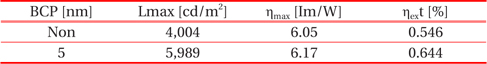
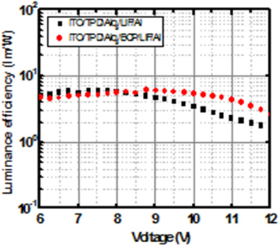
Figure 8 shows the luminous efficiency depending on the applied voltage for the devices with/without the electron-transport BCP layer. The maximum luminous efficiency of the device without BCP layer at a voltage of 7.75 [V] is about 6.05 [lm/W], and that of the device with BCP layer at a voltage of 8.75 [V] is approximately 6.17 [lm/W].
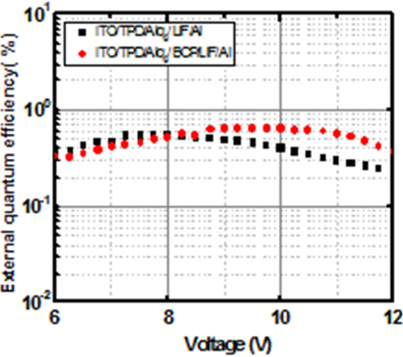
Figure 9 shows the external-quantum efficiency (ηext)-voltage characteristics for the devices with/without BCP layer. The maximum external-quantum efficiency for the device without BCP layer is approximately 0.546% at 7.75 V, and that for the device with BCP layer is approximately 0.644% at 9 V. Thus, the maximum luminous efficiency and the maximum external-quantum efficiency are improved by 2% and 18%, respectively, with the insertion of electron-transport BCP layer. These are summarized in Table 2.
[Table 2.] Maximum values of luminance and efficiencies for the devices with/without BCP layer.

Maximum values of luminance and efficiencies for the devices with/without BCP layer.
Electrical and optical characteristics of the OLEDs were studied in a device structure of ITO/TPD/Alq3/LiF/Al ITO/TPD/Alq3/BCP/LiF/Al in order to investigate the effect of electron-transport BCP layer. Since the BCP layer lowers the electron energy barrier, the electron transport is facilitated and the movement of hole is blocked as the applied voltage increases. This results in an increased recombination rate of holes and electrons. The study results indicate that the current density, luminance, luminous efficiency, and external-quantum efficiency are improved by approximately 22%, 50%, 2%, and 18%, respectively. Thus, it is expected that the electron-transport BCP material could contribute to the next generation of flat-panel display industry.