Recently, the high density memory has been developed by scaling down feature size. In order to increase the density and the speed while decrease the operating power of memory devices, methods to compensate for the decrease of gate width with high-dielectric materials must be explored. The reduction of the gate dielectric, commonly a SiO2 material, as the insulator layer of transistors causes serious problems in terms of leakage current and reliability. Therefore, a high-k material such as the TiO2 thin film has been studied to provide a substitute for SiO2 as the insulator layer of transistors. High-k thin films can be used as insulators for metal-insulator-metal (MIM) capacitors to increase the packing density of integrated circuits by increasing the dielectric constant of the insulators [1-3]. However, among new insulator candidates, TiO2 can achieve a high etch rate and a high selectivity for the sake of the throughput and reliability of the MIM capacitor.
Until now, the etch characteristics of TiO2 in inductively coupled plasma (ICP) and capacitively coupled plasma are not understood completely. The ICP source shows characteristics of high etch rate and high plasma density, as well as its own unique characteristics. Some of the basic properties and the process performance were previously reported [4-6]. However, new insulator candidates must comply with the device processing procedure. Among the high-k materials, TiO2 is good candidate because a high etch rate and high selectivity can be achieved for the necessary high throughput and reliability of the MIM capacitor.
In this study, TiO2 thin films were etched in an adaptively coupled plasma (ACP) system with various Cl2/Ar gas ratios. The etch characteristics of the TiO2 thin films were investigated in terms of the etch rate and the selectivity. The morphologies on the surface of the etched TiO2 thin films were investigated by atomic force microscopy (AFM). The chemical binding states on the surface of the etched TiO2 thin films were investigated by X-ray photoelectron spectroscopy (XPS). Field emission-scanning electron microscopy (FE-SEM) was used to investigate the etch profile.
The TiO2 thin films used in this work were deposited by plasma enhanced atomic layer deposition (PEALD). The substrate was a 6-in
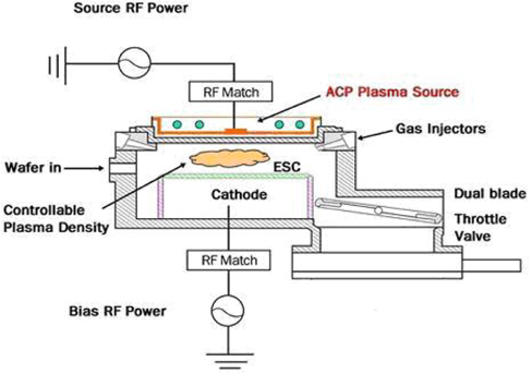
As shown in Fig. 1, the system consisted of multi-spiral coils and a bushing, and the coil antenna was located above a thick horizontal ceramic window. A 12.56 MHz RF power generator in the source power was connected to a coil antenna to generate the plasma. Another 13.56 MHz RF power generator in bias power was connected to the electrostatic chuck (ESC: 1500 V) to control the ion energy. This plasma source shows characteristics of both traditional sources of inductively coupled plasma (ICP) and capacitively coupled plasma (CCP), as well as its own unique characteristics [7,8]. The etch characteristics of the TiO2 thin films were investigated as a function of the Cl2/Ar gas mixing ratio. In addition, the etching of the TiO2 thin films was investigated by changing the etching parameters. The etch rate was measured by a surface profiler (KLA Tencor, α-step 500). The compositional changes on the surface of the etched TiO2 thin film were investigated using XPS (SIGMA PROBE, Thermo VG Scientific). The spectra were plotted by counting the photo electrons at kinetic energy intervals of 0.1 eV. The surface images of the etched TiO2 thin films was confirmed by using AFM (Dimension 3100, Veeco). All of the samples for the XPS and AFM analysis were bare TiO2 thin films that did not have any photoresist (PR) patterns, and the size of the samples was 1×1 cm2. The etching time was 10 sec. The etching profile of the cross-section was characterized using FE-SEM (Sirion 400, FEI). The TiO2 thin films used for measuring the etch rate and etching profile did have a PR (SS03A9) pattern. The width and thickness of the PR pattern were 1.5 μm and 1.02 μm, respectively.
For the etch characterization of the TiO2 thin film in the ACP system, the etch characteristics of the TiO2 thin film was systematically investigated as a function of the Cl2/Ar gas mixing ratio, source power, bias power, and process pressure. Generally, the combination of Cl2 and Ar enhances the etch rate of metal-oxide materials by forming volatile etch by-products, such as ClOx and metal-chlorides. Otherwise, the etch rate is decreased by forming non-volatile etch by-products of ClO [9-10]. If Cl2O3 is accumulated on the surface, this layer precludes any chemical reactions between Cl and metals [11]. The steady-state rate of the chemical etch pathway (ERch) is equal to (1-θ)γchSClГCl+(1-θ)YSГAr+ [12], where Г is fluxes of species to the etched surface, γch is the probability of chemical interaction, SCl is the sticking probability of atoms. θ is the fraction of surface active sites occupied by nonreactive species and determined by the balance between the rates of the chemical reaction (which fills the surface with low volatility reaction products) and the ion stimulated desorption [12].
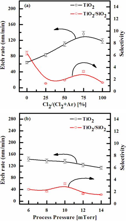
Fig. 2(a) shows the etch rate of the TiO2 thin film as a function of the Cl2/Ar gas mixing ratio was measured when the total flow rate was fixed at 100 sccm. The other process parameters condition was maintained as shown in the Table 1, respectively. As the Cl2 content in the Cl2/Ar gas plasma increases from 0% to 75%, the etch rates of the TiO2 thin films increase from 64±5 nm/min to 136±5 nm/min. When the Cl2 content increased over 75%, the etch rate of TiO2 thin film decreases. As the Cl2 content in the Cl2/Ar gas plasma increases from 0% to 75%, the selectivity, which is the etch rate ratio, of TiO2 to SiO2 decreases from 6.4 to 3.37. The effect is because SiO2 is reacts better than TiO2 when Cl2 contents increased. Cl2-based plasma etching shows SiO2 to be more effective than TiO2 in etching. The maximum etch rate of the TiO2 thin film was 136 nm/min, at a Cl2/(C12+Ar) ratio of 75%. The comparisons on etch rates of the TiO2 thin film in Cl2-based plasma shows that chemical etching is more effective than physical sputtering [13] TiO2 thin film etching in chlorine-based plasma is well known to produce highly volatile by-products such as Ti-Cl4. The evident enhancement on etch rate of the TiO2 thin film in the pure Cl2plasmas suggests that the chemical etch pathways provided by the Cl-atoms are the dominant mechanism for the given set of input process parameters. In the case of physical sputtering of TiO2 thin films, we expect the contribution of this pathway to be much lower than ion-assisted chemical reactions. In Cl2-based plasma, increasing Cl2 content up to 75% increases etch rate via two different mechanisms: (1) accelerated chemical reactions by the ion-stimulated desorption of the reaction products and (2) increasing the contribution of physical sputtering. Nevertheless, when the Cl2 content exceeds 75%, the etch rate begins to decline due to the interruption of physical sputtering. For a given range of experimental conditions, chemical reactions were more effective than the physical etch pathway [11,12]. Fig. 2(b) shows the etch rate of TiO2 thin film as a function of the process pressure in the Cl2/Ar (75%:25%) plasma. As the process pressures increased from 6 mTorr to 14 mTorr, the etch rates of the TiO2 thin film decreased from 144±5 nm/min to 114±5 nm/min. As the process pressure increases from 6 mTorr to 14 mTorr, the selectivity (or the etch rate ratio) of TiO2 to SiO2. O2 tends to be maintained in all sections. The effect of process pressure may be explained as follows: An increase in process pressure at fixed Cl2/Ar mixing ratio leads to an increase in both density and flux of fluorine atoms on the etched surface, but causes a decrease in ion flux and mean ion energy. As a result, the chemical etch pathway tends to accelerate, however, ion stimulated desorption of reaction products results due to a decreased fraction of free surface acceptable for chemical reaction. Similar to the effect of the gas mixing ratio discussed above, these two opposing factors produce non-monotonic behavior of the etch rate.
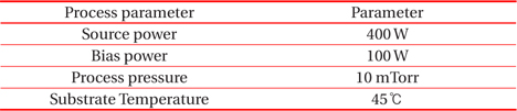
[Table 1.] The input plasma parameters.

The input plasma parameters.
We hypothesize that molecular bonds were broken by ion bombardment on the surface of the TiO2 thin film. Frequent chemical reactions in the plasma were facilitated by the higher ion density and the increased number of broken molecular bonds. This conclusion is in good agreement with the data shown in Fig. 2(a) and Fig. 2(b) [9-12].
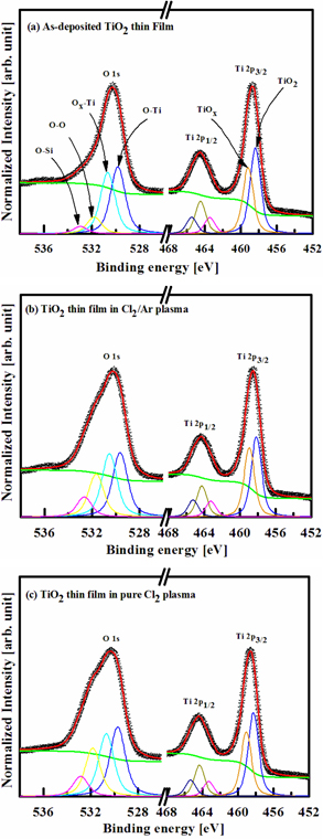
For more detailed investigation of the chemical reaction on the etched surfaces, XPS analysis was carried out. We compared the differences between the chemical reactions on the surface of the etched TiO2 thin film and on the surface of the as-deposited TiO2 thin film. We also compared the differences between the peaks from the as-deposited TiO2 thin film and the etched TiO2 thin films in order to evaluate the changes of the chemical shift. The input plasma parameters were as follows at the Table 1.
Figure 3 shows the Ti 2p and O 1s XPS narrow-scan spectra on the surface of the etched TiO2 thin film as a function of the Cl2/Ar gas mixing ratio. As shown in Fig. 3(a), there are strong peaks at 464.34 eV and 458.8 eV, which correspond to Ti 2p1/2 and Ti 2p3/2 in the TiO2 thin film. These peaks were shifted toward a low binding energy and the maximum deviation was about Δ 0.3 eV when the TiO2 thin films were exposed in Cl2/Ar plasma. This chemical shift indicates that Ti chemically reacted with Cl radical at the surface [13-15]. The intensity of this peak increases slightly with the Cl2/Ar (75%:25%) plasma, as shown in Fig 3(b), this changes of intensity can be related to the signal from the Ti-Ox bond, which was deconvoluted as shown in Fig. 3. These peaks were shifted toward the higher binding energy and the maximum deviation was about Δ 0.1 eV when TiO2 thin films were exposed in pure Cl2plasma, as shown in Fig. 3(c). From these facts, we can conclude that the Ti-O bonds are effectively destroyed by the Cl+ ion bombardments, which is in good agreement with the etch mechanism proposed above and the O 1s XPS narrow-scan spectra on the surface of the etched TiO2 thin film as function of the Cl2/Ar gas mixing ratio. As shown in Fig. 3(a) as-deposited, there is a strong peak at 530.2 eV, which corresponds to the O 1s in TiO2 thin film. The O 1s peak of as-deposited TiO2 thin film showed a single peak. This peak was composed of four maximums at 533 (O-Si), 531.8 (O-O), 530.65 (Ox-Ti) and 529.8 eV (O-Ti). In order to investigate the chemical states of the surface, the O 1s peaks were deconvoluted. As shown in Fig. 3(b) and (c), the O 1s peak was deconvoluted into four peaks, which were determined to correspond to the oxygen and/or hydroxyl group on the surface in the Cl2/Ar plasma and the pure Cl2: O-Si bond (532.7±0.3 eV), O-O bond (531.65±0.15 eV), Ox-Ti bond (530.55±0.1 eV), and O-Ti bond (529.65±0.15 eV). The confirmation of this is that the intensity of the peak centered at 530.2 eV was constant and was not dependent on the film treatment conditions [13,14].
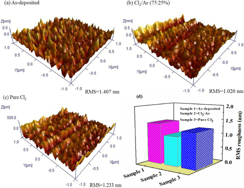
As shown in Fig. 4, in order to clarify the etch mechanism further in terms of surface morphology, the etched TiO2 thin films by the pure Cl2 and the Cl2/Ar (75%:25%) plasma were investigated by AFM observation as function of the Cl2/Ar gas mixing ratio. The input plasma parameters were as follows as shown in the Table 1. For comparison, on the surface of the as-deposited TiO2 thin film is also measured and exhibits a roughness of about 1.407 nm (Fig. 4(a) as-deposited). For the pure Cl2plasma and etching by Cl2/Ar (75:25%) plasma, the roughness is approximately 1.233 nm and 1.020 nm, respectively, [Fig. 4(b) Cl2/Ar (75%:25%) and (c) pure Cl2) due to the re-deposition effect. From the summarized roughness result shown in Fig. 4(d), decreasing the Cl2 content in the Cl2/Ar mixture brought about the formation of a coarse surface.
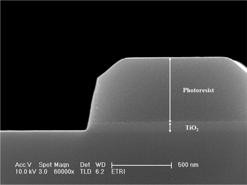
Figure 5 shows the cross sectional SEM images of the TiO2 thin film after etching in Cl2/Ar (75%:25%) plasma at a fixed condition shown in the Table 1 and the etching time was 30 sec. As shown in Fig. 5, the cross-sections of the PR and TiO2 thin films were obtained with a PR mask. The experimental results showed that the vertical etching profile after plasma etching of the TiO2 thin film was associated with Cl-radicals, due to the high etch rate of the TiO2 thin film.
In this paper, the etch characteristics of TiO2 thin films were investigated by measuring the etch rates under the varying input parameters using an ACP system. The maximum etch rate of the TiO2 thin film was 136.4 nm/min at a Cl2/(Cl2+Ar) gas ratio of 75%. As the fraction of Cl2 in the Cl2/Ar plasma was increased from 0% to 75%, the etch rate of the TiO2 thin film increased. However, the etch rate of the TiO2 thin film decreased with the further addition of Cl2 gas. The etch rates of the TiO2 thin films increased with increasing source power and bias power, but decreased with increasing process pressure. Ion bombardment was required, due to the relatively high volatility of the by-products formed during etching by the Cl2/Ar plasma. The chemical states on the surface of the etched TiO2 thin films were investigated using XPS. The etch characteristics of the TiO2 thin film can be explained as follows: Ti interacted with the Cl-radicals in the Cl2 containing plasmas to form the high volatile TiClx by-products, which can be effectively removed with the help of ion bombardment. The results agreed well with the general energy dependency of the ion-enhanced chemical etching yields.