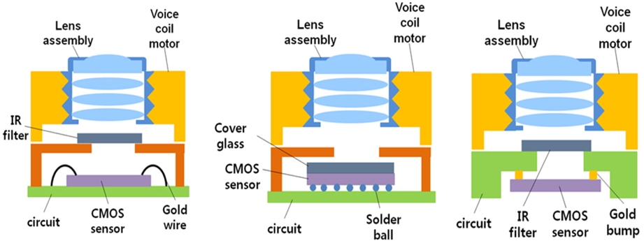
In general, there are three types of packaging methods for phone camera lens modules: the wire-bonding, solder-ball, and flip-chip methods. The wire-bonding method, as illustrated in Fig. 1(a), affords high productivity and low cost, but it has a problem with compactness. The method using solder balls, as illustrated in Fig. 1(b), can reduce the number of packaging steps, but the manufacturing cost is higher than for the other methods. Finally, flip-chip packaging exhibits an advantage in compactness. Recently the mobile phone industry has required extremely thin phones, and flip-chip packaging is considered to be best.
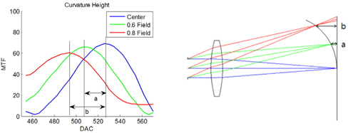
After packaging, the modulation transfer function (MTF) of each phone camera module is measured, to verify the performance of the module. The MTF is an optical resolution criterion, particularly for image-forming systems [1-5]. It has perhaps the most factors of all optical criteria. These factors include lens aberration (e.g. spherical aberration, astigmatism, coma, and field curvature), manufacturing and assembly errors (e.g. de-centering, irregularity, tilt, thickness, air gap, and refractive index), the testing environment (e.g. light-source intensity, color temperature, test alignment, and test-chart quality), and so on. The critical factor for MTF degradation during assembly of a mobile phone camera moduleis the optical tilt; however, it can be overcome using an active alignment scheme that aligns the optical axis and the CMOS image sensor to be perpendicular, prior to attaching them. After the optical tilt has been resolved, the second critical factor is the field curvature. To verify the influence of these two dominant errors (tilt and field curvature), a typical phone camera module was selected, and its MTF degradation was simulated at a spatial frequency of 105 lp/mm.
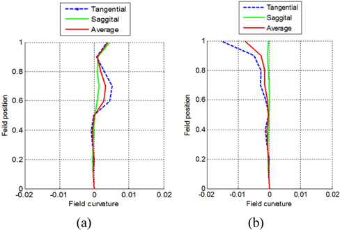
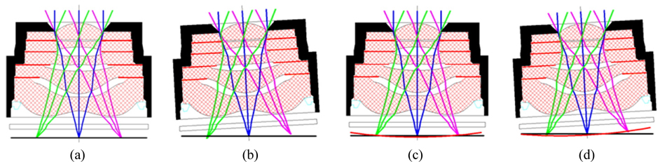
Figure 3 presents the models of (a) no error, (b) tilt only, (c) field curvature only, and (d) coupled error. A 0.3° tilt angle and a field curvature 5 μm in height were considered in the simulation, because these numbers often appear in real manufacturing processes. In the worst-case scenario, MTF degradation can be up to 35% at Nyquist frequencies over 4 [6], as depicted in Fig. 4(d). However, after active alignment is adopted, the tilt error can be significantly reduced. Nevertheless, it remains difficult to achieve a high resolution in the phone camera module due to the field-curvature effect. A 5-μm curvature height at 0.6 field off-axis produces approximately 15% MTF degradation, which causes yield loss, as depicted in Fig. 4(c). This situation was also investigated using experiments. The lens assembly was intentionally tilted by almost 0.3°, and approximately 5 μm of curvature height was introduced via adjusting the space between each lens. The actual measured MTF degradation is presented in Fig. 5. It should be noted that the experimental results are similar to the simulations.
To address this problem, a new method is proposed that reduces the total amount of field curvature of the phone camera module with a curved CMOS image sensor, through optimizing the distance between the lens elements. In the phone camera industry, this distance is called the air gap. The field-curvature model is derived in Section II. The simulations and experimental results are shown in Section III and IV respectively.
II. LENS FIELD CURVATURE AND ITS CORRECTION
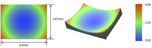
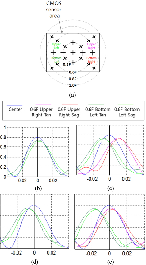
Through failure analyses of the MTF that results from field curvature, a lens was detached from the camera module and the field curvature of the lens was measured. It was found to be less than the field curvature of the camera module, which was a lens with a CMOS image sensor. Although the optical system was the same, the curvature height was approximately 5 μm worse when the CMOS sensor was attached, as depicted in Fig. 6. To determine the extra field curvature, the flatness of the CMOS image sensor was measured using a commercial phase-shifting interferometer [7-10], and the sensor was found to have spherical curvature, as illustrated in Fig. 7.
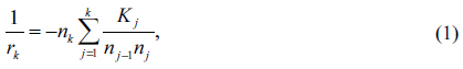
Lens designers usually consider a flat image plane while attempting to minimize the field curvature. However, the actual measurement data revealed that the CMOS image sensors usually were not flat, but curved, with an average of 3-5 μm in the full-field position. This is a considerable amount if the direction of curvature is not coincident between the lens assembly and the CMOS image sensor, because it is natural that the curvature sag increases at farther fields for both lens and sensor. It also increases with the square of the field angle or theimage height. Therefore, the curvature direction must be made to coincide at farther fields. The field curvature is one of Seidel’s aberrations [11] where the focal plane is not flat but curved, and it causes image-resolution imbalance along the image field. The surface formulation, according to the Petzval theorem, is as follows:

where

However, it is not possible to affect the Petzval sum through redistributing the surface power while maintaining the net power. It is not dependent on the lens bending. For a thick lens, the total power is

This indicates that the Petzval sum is reduced when the power distribution is
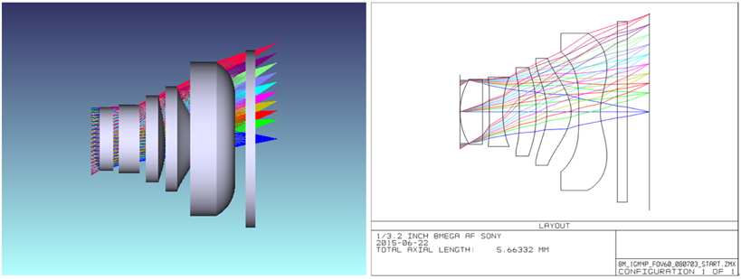
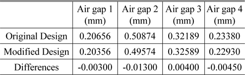
To verify the proposed method, simulations were undertaken using the ZEMAX software [13] with a common mobile phone lens. The specifications of the lens were construction using 1 glass mold and 4 plastic aspheric elements with an f-number of 2.4, an effective focal length of 4.89 mm, and a 60° field of view. The direction of the field curvature of the original design was opposite to that of the image sensor’s curvature. Although this lens had good MTF performance at the lens-only level, it resulted in MTF degradation with the image sensor, as described in the previous section. Air gaps 1 to 4 were optimized to change the direction of the lens’s field curvature by using a merit function regression method.
A previously reported merit function regression [14] was complicated and took a long time to optimize the posture and position of the lens, but the proposed optimization method can reduce the calculation time dramatically, since the field curvature mainly depends on the de-space (air-gap direction), and we included the constraint that each lens can only move along the optical axis. The optimized air-gap data are described in Table 1. The air gap was reduced to create a negative field curvature that corresponded to the sensor curvature’s direction, as depicted in Fig. 8.
[TABLE 1.] Air gap optimization
Air gap optimization
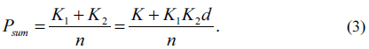
MTF simulation was also conducted. The lens with modified air gap showed field curvature at the 0.8 field, but that was compensated with a curved image sensor, as illustrated in Fig. 9.
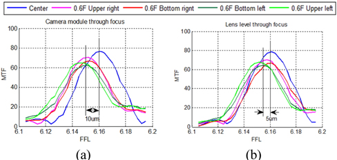
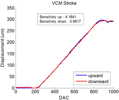
The curvature height, i.e. the differences in MTF peak position between the reference center position and other fields, can be calculated from the MTF through-focus data. The interpolation curve of the curvature height is the field curvature. The curvature height is expressed to the DAC (digital to analog conversion) in through-focus data because the driver IC (integrated circuit) signal for the autofocusing actuator is from the DAC; therefore, the laser distance metrology was applied to convert the DAC into the displacement.
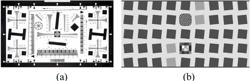
The lens MTF was measured using an Image Master HR tester in Trioptics [15], and the camera module MTF was measured according to the ISO-12233 method [16], as depicted in Fig. 11. The test chart was modified from the ISO-12233 chart by cropping it according to the sensor size ratio, selecting only the slanted edge features, and locating the specific field point, as depicted in Fig. 12. For this experiment the slanted edge was selected at the on-axis and four corners in the 0.6 field, and four other corners in the 0.8 field.
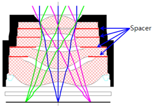
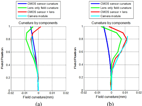
The film space is often used for several purposes in mobile phone lens manufacturing. It is a doughnut-shaped thin film between the lens elements. It vignettes [17] unexpected stray light, controls relative illumination, and controls the space between lenses. Referring to the simulation results, two lens samples were prepared: One had the same spacer thickness as the original lens design with a positive field curvature (which was in the opposite direction of the image-sensor curvature), and the other had a modified spacer thickness based on Table 1 with a negative field curvature (which was in the same direction as the image-sensor curvature). The lens field curvature of the prepared samples and sensor curvature were measured individually, before assembling them into the camera module. The two components were assembled with active alignment, minimizing the optical tilt. After assembling the lens and CMOS image sensor, the net field curvature at the camera module level was measured with the MTF through-focus data.
The field curvature of only the lens was of similar magnitude for both lenses; however, the net field curvature at the camera module level was significantly different. The field curvature was noticeably improved when the direction of the field curvaturecoincided with that of the image sensor. Furthermore, the camera module field curvature correlated well with the mathematical sum of the measured lens field curvature and sensor curvature. Table 2 demonstrates that the camera module field curvature could be degraded or improved according to the amount of CMOS sensor curvature. For example, if the direction of the lens curvature direction is opposite that of the sensor, the camera module field curvature worsened, +11.8 μm, compared to the lens field curvature of +7.3 μm, whereas the camera module field curvature was only -4.8 μm with a -9 μm lens field curvature when the curvature direction is the same as for the sensor.
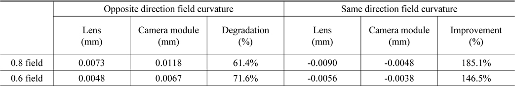
Improvement and degradation of camera module net field curvature in the region of interest
To obtain high yield for mobile phone camera module manufacturing, it is important to consider the curvature of the CMOS image sensor. Recently, high MTF specifications have been required at very far fields, such as 0.8 and beyond. The curvature increases in the far field; therefore, a lens designer should attempt to align the direction of the lens field curvature with that of the sensor curvature. In this paper that phenomenon was reported, and an effective and efficient solution via optimizing the lens air gap was proposed to control the lens field curvature without side effects. Using the newly proposed method, the net field curvature of the final phone camera module was as well compensated as the amount of the sensor curvature.