In each new technology generation, the amount of on-die memory cache increases to enhance the performance of modern microprocessors [1-3]. SRAM cell is the fundamental building block of on-chip memory cache. Reduced power supply and device threshold voltages degrade the data stability and write ability of SRAM cells with CMOS technology scaling. Furthermore, memory banks consume a significant amount of leakage power due to the large number of transistors [1-3,10-12,20]. Novel SRAM cells are highly desirable for achieving more compact, robust, and energy-efficient memory circuits.
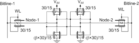
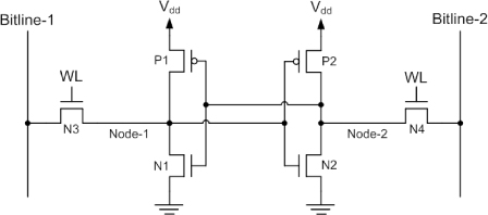
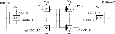
Current industry standard SRAM cells are composed of six transistors (6T) as shown in Fig. 1. The data storage nodes (Node-1 and Node-2) of six transistor (6T) SRAM cells are directly accessed by the bitlines during read operations [1-3], and thereby the voltages of the data storage nodes are disturbed. Weakening the bitline access transistors is preferable for providing enhanced data stability during read operations in conventional 6T SRAM cells [1-3,8]. Alternatively, strengthening the bitline access transistors is desirable for achieving faster data transfer and wider voltage margin during write operations [1-3]. Conflicting design requirements exist for achieving stronger read data stability as well as faster and easier write ability in conventional 6T SRAM cells.
Two new techniques for enhancing the read data stability without degrading the integration density and write ability in 6T SRAM cells are presented in this paper. The strengths of the bitline access transistors are dynamically adjusted during read and write operations with an asymmetric device structure in the new SRAM cells. Stronger read data stability is thereby achieved without degrading write ability with the proposed asymmetric gate-underlap engineering techniques. The read static noise margin of the new SRAM cells with asymmetric bitline access transistors are enhanced by up to 71.6% and the leakage power consumption is reduced by as much as to 15.5% without increasing the silicon area as compared to the conventional symmetric 6T SRAM cells in a 15 nm FinFET technology.
This paper is organized as follows. The conventional SRAM cell composed of six symmetric FinFETs is described in Section 2. In Section 3, SRAM cells with asymmetric FinFETs are presented. SRAM cells are characterized and compared under identical silicon area constraint in Section 4. SRAM cells are compared under similar data stability constraint in Section 5. Impact of process parameter fluctuations on electrical characteristics of memory circuits are discussed in Section 6. The paper is summarized in Section 7.
2. CONVENTIONAL SYMMETRICAL Six-FinFET SRAM CELL
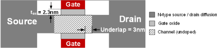
Transistors used in the conventional SRAM cell are symmetrically gate-to-source and gate-to-drain underlapped six FinFETs [17,22,23,31-33]. The symmetrically gate-underlapped FinFETs (FinFET-Sym) are designed and optimized to match the International Technology Roadmap for Semiconductors (ITRS) [5] projections for 15 nm FinFET technology node. The temperature for device simulation is 25℃ [5]. Atlas 2D simulator [6] is used to characterize the SRAM cells. Quantum correction, carrier-carrier scattering, surface scattering, carrier velocity saturation, field dependent mobility, concentration dependent mobility, and temperature dependent mobility models are used in the simulation. The gate length, fin thickness, and fin height of transistors are 15 nm, 6 nm, and 15 nm, respectively. The gate work-functions of the n-type and p-type FinFETs are 4.46 eV and 4.88 eV, respectively. Equivalent gate oxide thickness is 0.7 nm [5] (1.9 nm HfO2 + 0.4 nm SiO2). Gaussian source / drain doping profile is assumed with peak doping concentration and characteristic length [6] of 2×1020 cm−3 and 2 nm, respectively. The profile of the optimized n-type FinFET-Sym is shown in Fig. 2. The on-current and off-current that are produced by the minimum size (single-fin) n-type FinFET are 1,756 μA/μm and 82 nA/μm, respectively. The p-type FinFETs are designed to produce half of the on-current as compared to the n-type FinFETs in this study.
The conventional SRAM cell with six symmetric FinFETs (SRAM-Sym) is shown in Fig. 3. The operation of SRAM-Sym is as follows. The wordline signal (WL) of an un-accessed cell is maintained at 0 V. The bitline access transistors are cut-off. The data is maintained by cross-coupled inverters in an un-accessed SRAM cell. The bitlines are pre-charged to Vdd prior to a read operation. WL transitions to Vdd to initiate the read operation. The bitline access transistors are turned-on. Provided that a “0” is stored on Node-1, Bitline-1 is discharged through N3 and N1. The voltage level of Node-1 is raised above 0 V due to the voltage division between the bitline access and pull-down transistors. The stored data is disturbed due to the direct read access mechanism in a symmetric 6T SRAM cell. In order to maintain sufficient read data stability with 6T SRAM cells, the bitline access transistors are required to be weaker compared to the pull-down transistors in cross-coupled inverters [1-3].
Prior to a write operation, depending on the incoming data, one of the bitlines of each accessed column of the memory array is discharged to 0 V. The wordline signal (WL) transitions to Vdd to initiate a write operation. The bitline access transistors are turned-on. Provided that a “0” is forced from Bitline-1 to Node-1 where a “1” was previously stored, the bitline access transistor (N3) competes with the pull-up transistor (P1) to discharge Node-1 from Vdd to 0 V. In order to achieve faster data transfer and wider voltage margin during write operations, the bitline access transistors should be stronger as compared to the pull-up transistors in cross-coupled inverters. While the bitline access transistors are desirable to be weaker for achieving stronger read data stability, the bitline access transistors are desirable to be stronger for providing wider voltage margin during write operations. Conflicting design requirements exist for achieving stronger read data stability and faster/easier write ability in 6T SRAM cells with symmetrical bitline access transistors.
3. FinFET SRAM CELLS WITH ASYMMETRICAL BITLINE ACCESS TRANSISTORS
Three different SRAM cells that employ asymmetrical transistors are presented in this section. Asymmetrically gate overlap / underlap engineered FinFET is introduced in Section 3.1 A previously published purely asymmetric six-FinFET SRAM cell and a novel hybrid six-FinFET SRAM cell with asymmetrically gate overlap / underlap engineered transistors are described in Section 3.2 An alternative hybrid six-FinFET SRAM cell with asymmetrically gate-underlapped bitline access transistors is proposed in Section 3.3.
3.1 Asymmetrically gate overlap / underlap engineered FinFETs
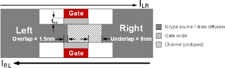
The cross sectional view of an n-type asymmetrically gate overlap / underlap engineered FinFET (FinFET-Asym1 [13]) is shown in Fig. 4. The left side of the channel is overlapped while the right side is underlapped by the gate terminal in the asymmetrical FinFET-Asym1 structure [13].
The on-current that is produced by an asymmetric FinFET varies depending on the direction of current flow. When the voltage level of the left electrode is higher than the right electrode, the right electrode is the source of charge carriers while the left electrode is the drain terminal in an n-type FinFET-Asym1. The underlap region on the source side (right side) is far away from the gate. The fringing electric field that emerges from the gate cannot induce sufficient number of carriers in the underlap region on the source side. The channel resistance is therefore increased. Due to the asymmetric design of FinFET-Asym1, the on-current flowing from the left to the right (ILR) is reduced as compared to a symmetric FinFET. Suppressing ILR of bitline access transistors is desirable for achieving stronger data stability during read operations in 6T SRAM cells.
Alternatively, when the voltage level of the right electrode is higher than the left electrode, the left electrode is the source of charge carriers while the right electrode is the drain terminal in an n-type FinFET-Asym1. Since the left side of the device is gate overlapped, a higher concentration of carriers is induced in the channel area with stronger field-effect. Drain induced depletion on the right side of the channel further reduces the channel resistance at the gate-underlap region. As illustrated in Fig. 4, the on-current flowing from the right side of the device to the left side (IRL) is significantly higher as compared to the left-to-right on-current (ILR) due to the asymmetrical design of FinFET-Asym1. Maintaining high IRL in the bitline access transistors is critical for achieving faster data transfer and wider voltage margin during write operations in 6T SRAM cells.
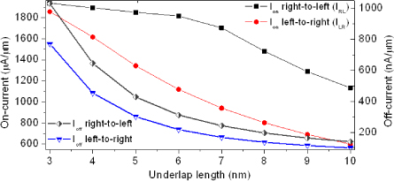
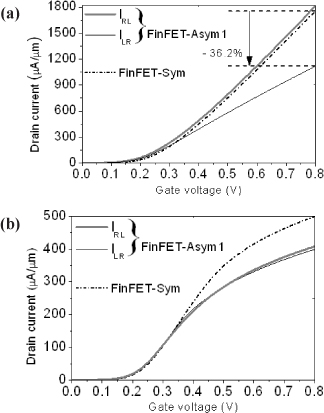
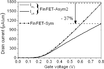
The gate overlap length is 10% of the nominal gate length in FinFET-Asym1 [1-3]. The underlap on the right side of the device is increased from 3 nm to 10 nm for lowering ILR as much as possible while maintaining IRL similar to the on-current of the optimum FinFET-Sym in this study. The right-to-left on-current (IRL) is similar to the on-current of the optimum FinFET-Sym when the right underlap and left overlap lengths are 6 nm and 1.5 nm, respectively, as shown in Fig. 5. The preferred underlap and overlap lengths in FinFET-Asym1 are therefore 6 nm and 1.5 nm, respectively. Due to shorter effective channel length in FinFET-Asym1, the off-current that is flowing from right-to-left is however increased by 3.8 times as compared to FinFET-Sym. Similarly, the off-current that is flowing from left-to-right is increased by 2.7 times with FinFET-Asym1 as compared to FinFET-Sym. The FinFET-Asym1 profile that is used for SRAM cell design in this study is shown in Fig. 6. The saturation region drain current of FinFET-Asym1 and FinFET-Sym are compared in Fig. 7(a). ILR that is produced by FinFET-Asym1 is 36.2% lower as compared to the on-current that is produced by FinFET-Sym.
3.2 SRAM cells with asymmetrically gate overlap / underlap engineered FinFETs
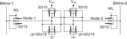
By employing asymmetrically gate overlap / underlap engineered FinFETs (FinFET-Asym1), a purely asymmetric six-FinFET SRAM cell (SRAM-Asym) is proposed in a previous study [13]. The strength of bitline access transistors are dynamically adjusted during read and write operations with this technique. SRAM-Asym is shown in Fig. 8. All of the transistors in SRAM-Asym are asymmetrical (FinFET-Asym1). The gate-underlapped sides (right sides) of the pull-up, pull-down, and bitline access transistors are connected to the data storage nodes. The gate overlapped sides of the bitline access transistors are connected to the bitlines. The gate overlapped sides of the pull-up and pull-down transistors in cross-coupled inverters are connected to Vdd and ground, respectively.
The pull-down transistor that is holding a “0” operates in the linear region during read operations in a 6T SRAM cell. Higher linear region on-current is desirable in the pull-down transistors of cross-coupled inverters for providing stronger data stability during read operations. The linear region drain currents of FinFET-Asym1 and FinFET-Sym are compared in Fig. 7(b). The linear region ILR and IRL that are produced by FinFET-Asym1 are 20.1% and 18.2% lower, respectively, as compared to the linear region on-current that is produced by FinFET-Sym. SRAM-Asym therefore cannot enhance the data stability significantly despite having weaker bitline access transistors as compared to the symmetrical memory cells. Furthermore, the leakage currents that are produced by the asymmetrical transistors in cross-coupled inverters are higher as compared to the symmetrical transistors. SRAM-Asym therefore consumes significant leakage power in the idle mode.
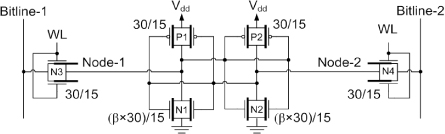
Symmetrical FinFETs are preferable in cross-coupled inverters for producing lower leakage currents in an SRAM cell. Alternatively, asymmetrical transistors are preferable for bitline access to achieve stronger data stability during read operations. Based on these observations, a novel hybrid SRAM cell (SRAM-Hybrid1) that employs both symmetrical and asymmetrical transistors is proposed in this paper as shown in Fig. 9. Asymmetrically gate overlap / underlap engineered FinFETs (FinFET-Asym1) are employed for bitline access. Alternatively, cross-coupled inverters are implemented with symmetric FinFETs (see Fig. 2 for the FinFET-Sym profile) in order to enhance the read data stability and suppress the subthreshold leakage currents with this new technique as compared to the previously published purely asymmetric SRAM-Asym.
The operations of SRAM-Asym and SRAM-Hybrid1 are similar. The bitline access transistors are turned-on to initiate a read operation. The read current (ILR) that flows from the bitline to the node that stores a “0” is weakened with FinFET-Asym1 compared to a symmetric transistor during read operations. Furthermore, the symmetric pull-down transistor that stores a “0” in SRAM-Hybrid1 is stronger than the asymmetric pull-down transistors in SRAM-Asym during read operations. The voltage disturbance on data storage nodes is therefore suppressed in SRAM-Hybrid1 as compared to SRAM-Asym and SRAM-Sym. The read data stability is thereby enhanced with SRAM-Hybrid1 as compared to both SRAM-Asym and SRAM-Sym.
The bitline access transistors are turned-on during write operations. Provided that a “0” is forced from Bitline-1 to Node-1 where a “1” was previously stored, the bitline access transistor (N3) competes with the pull-up transistor (P1) to discharge Node-1 from Vdd to 0 V. The gate overlapped terminal of N3 (the left side of the asymmetrical FinFET-Asym1 in Fig. 6) that is connected to the bitline acts as the source of electrons. The channel series resistance of the asymmetrical bitline access transistor is reduced due to stronger field-effect and channel inversion at the source end. The write currents (IRL) that flow from the data storages node to the bitlines in SRAM-Asym and SRAM-Hybrid1 are similar to SRAM-Sym. The asymmetric pull-up transistor that is holding a “1” is weaker in SRAM-Asym as compared to other SRAM cells. The write voltage margin of purely asymmetrical SRAM-Asym is therefore wider as compared to SRAM-Sym and SRAM-Hybrid1.
3.3 Hybrid FinFET SRAM cell with asymmetrically gate-underlap engineered bitline access transistors
The new hybrid asymmetrical FinFET SRAM cell (SRAM-Hybrid1) that is presented in Section 3.2 is effective in achieving stronger data stability and write ability. Due to shorter effective channel length, however, FinFET-Asym1 produces higher bitline leakage currents as compared to symmetrical FinFETs in the idle mode. Larger bitline leakage currents increase the power consumption in idle mode. Furthermore, larger bitline leakage currents degrade the read speed and may cause read failure particularly at ultra-low power supply voltages [28]. An alternative hybrid FinFET SRAM cell with asymmetrically gate-underlap engineered bitline access transistors is proposed in this section to suppress the bitline leakage currents while providing similar read data stability and write ability as compared to SRAM-Hybrid1.
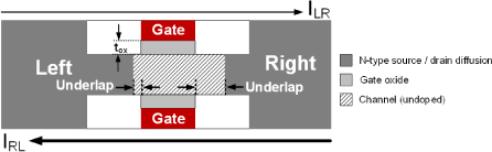
The cross-sectional view of an n-type asymmetric gate-underlap engineered FinFET (FinFET-Asym2) is shown in Fig. 10. The underlap on the right side is longer as compared to the left side in an asymmetric FinFET-Asym2 [14]. When the voltage level of the left terminal of FinFET-Asym2 is higher than the right terminal, the on-current flowing from the left side of the device to the right side (ILR) is reduced due to the increased series resistance of the channel with the longer underlap region on the right side of the device. Suppressing the ILR of bitline access transistors is desirable for providing stronger data stability during read operations in 6T SRAM cells. Alternatively, when the voltage level of the right electrode is higher than the left electrode, the on-current flowing from the right side of the device to the left side (IRL) is increased due to the reduced resistance of the channel. As illustrated in Fig. 10, IRL is significantly larger compared to ILR due to the asymmetrical design of FinFET-Asym2. Maintaining high IRL in the bitline access transistors is critical for achieving faster data transfer and wider voltage margin during write operations in 6T SRAM cells.
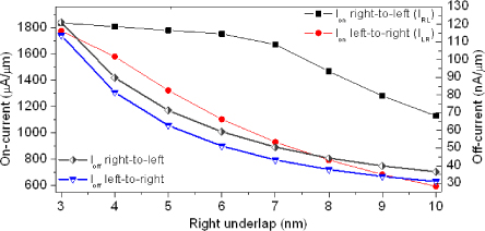
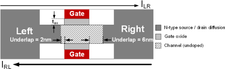
The underlap length on the left side of FinFET-Asym2 varies from 0 nm to 3 nm in this device optimization study. For each underlap length on the left side, the underlap length on the right side is increased from 3 nm to 10 nm to lower ILR as much as possible while maintaining IRL similar to the on-current of FinFET-Sym. The right-to-left on-current (IRL) is similar to the on-current of FinFET-Sym when the right underlap length is 6 nm with a left underlap of 2 nm, as shown in Fig. 11. The preferred underlap lengths on the left and right sides are therefore 2 nm and 6 nm, respectively, in the FinFET-Asym2 profile that is used for SRAM cell design in this study. Due to longer effective channel length, the left-to-right off-current that is produced by FinFET-Asym2 is 37.8% lower than the current that is produced by FinFET-Sym. Alternatively, the right-to-left off-current that is produced by FinFET-Asym2 is 27.9% lower than the current that is produced by FinFET-Sym, as shown in Fig. 11. The saturation region currents that are produced by FinFET-Asym2 and FinFET-Sym are compared in Fig. 12. The left-to-right on-current (ILR) that is produced by FinFET-Asym2 is 37% lower as compared to FinFET-Sym.
The device profile of the asymmetrically gate-underlap engineered FinFET (FinFET-Asym2) that is used for SRAM cell design in this study is shown in Fig. 13. The new low-leakage six-FinFET hybrid SRAM cell (SRAM-Hybrid2) that employs asymmetrically gate-underlap engineered FinFETs (FinFET-Asym2) as the bitline access transistors, is shown in Fig. 14. The shorter gate-underlapped sides are connected to the bitlines while the longer gate-underlapped sides of the asymmetrical bitline access transistors (see Fig. 13 for the FinFET-Asym2 profile) are connected to the data storage nodes. The cross-coupled inverters of SRAM-Hybrid2 are implemented with symmetrical FinFETs (see Fig. 2 for the FinFET-Sym profile).
The operation of SRAM-Hybrid2 is similar to SRAM-Asym and SRAM-Hybrid1. During read operations, the read current flows from the bitline to the node that stores a “0” inside the memory cell. Due to the higher series resistance of the channel, the bitline access transistor is weakened during read operations. The read data stability is thereby enhanced with the asymmetrically gate-underlap engineered bitline access transistors as compared to the six-FinFET SRAM cells with symmetrical bitline access transistors.
During write operations, the write current flows from the node that stores a “1” inside the memory cell to the discharged bitline. The write current is significantly higher than the read current in SRAM-Hybrid2. The transfer of new data into the SRAM cell is thereby facilitated with the proposed asymmetrically gate-underlapped bitline access transistors. Furthermore, the bitline leakage current that is produced by the hybrid asymmetrical SRAM-Hybrid2 is suppressed as compared to the purely asymmetrical SRAM-Asym, hybrid asymmetrical SRAM-Hybrid1, and symmetrical SRAM-Sym.
Fabrication of asymmetrically gate-underlapped single gate MOSFETs are reported in [15] and [16] by Advanced Micro Devices (AMD) Incorporation and NEC Corporation, respectively. Prior to the source / drain doping, spacers are etched asymmetrically on the two opposite sides of the gate [15,16]. Similar process can be used to fabricate asymmetrically gate-underlapped FinFETs. Furthermore, fabrication of symmetrically gate-underlapped transistors are reported in [17,25-27]. Prior to the source / drain doping, SiO2 or SiN spacers are formed on both sides of the gate. The underlap length is controlled by the width of the gate spacer. Uniformity of the gate spacer is critical to avoid significant fluctuations in the electrical characteristics of devices. Uniform deposition of gate spacers is demonstrated with the fabrication of FinFETs with symmetrical gate-underlaps in [17]. Very large-scale integration of symmetrically and asymmetrically gate-underlapped FinFETs for the realization of the hybrid memory circuits proposed in this paper is therefore feasible.
4. CHARACTERIZATION OF FinFET SRAM CIRCUITS WITH IDENTICAL SILICON AREA CONSTRAINT
The layout area, read data stability, write voltage margin, hold data stability, leakage power consumption, and data access (read and write) delays of the conventional symmetrical SRAM-Sym, the previously published purely asymmetrical SRAM-Asym, the first proposed hybrid asymmetrical memory cell (SRAM-Hybrid1), and the second proposed hybrid asymmetrical memory cell (SRAM-Hybrid2) are compared in this section at the typical process corner of a 15 nm FinFET technology. Three different β ratios of 1, 2, and 3 are considered for providing different levels of data stability and memory integration density in this study. Due to high power density of SRAM banks in modern high performance microprocessors, the temperature of memory cache is assumed to be 90℃ [24] in this study. The power supply voltage is 0.8 V.
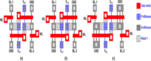
Layouts of different SRAM cells are shown in Fig. 15. The layout design rules of SRAM cells are provided in [1]. The fin spacing of multi-fin transistors is assumed to be 15 nm [18] for maximizing the memory integration density. Prior to the source / drain doping, spacers are formed on both sides of the gate in source / drain extension regions. The underlap lengths are controlled by the width of the sidewall spacers. After the source / drain ion implantation, devices are covered by dielectric for further processing. Sidewall spacers do not increase the length of source / drain extensions as long as the underlap lengths are shorter than the extension regions. The gate underlap lengths of all the transistors are shorter than the source / drain extensions in this study. The lengths of the source and drain extensions in different FinFETs are therefore identical. The device footprints of FinFET-Sym, FinFET-Asym1, and FinFET-Asym2 are equal. The employment of asymmetric transistors therefore does not alter the layout area as compared to the symmetrical SRAM cells. The layout areas of different SRAM cells (with the same β ratio) are identical. The minimum-sized SRAM cell area is 0.038 μm2 .
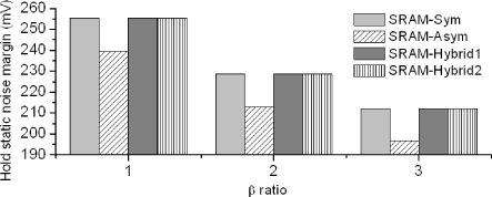
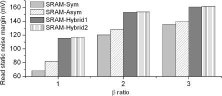
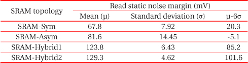
The data stability of an SRAM cell is characterized by the read static noise margin (RSNM) [1-3]. The RSNM of FinFET SRAM cells with different β ratios are shown in Fig. 16. The read currents (ILR) that are produced by the bitline access transistors (FinFET-Asym2 and FinFET-Asym1) in SRAM-Hybrid2 and SRAM-Hybrid1 are lower as compared to SRAM-Sym. Furthermore, the pull-down transistors (FinFET-Sym) in cross-coupled inverters of SRAM-Hybrid2 and SRAM-Hybrid1 have larger linear region on-currents as compared to the purely asymmetrical SRAM-Asym. The read static noise margins of the proposed hybrid asymmetrical SRAM cells are enhanced by up to (depending on the β-ratio of SRAM cells) 71.6% and 42.7% as compared to the symmetric SRAM-Sym and previously published purely asymmetric SRAM-Asym, respectively. The two hybrid asymmetric memory cells (SRAM-Hybrid1 and SRAM-Hybrid2) offer similar data stability (difference less than 2%).
The hold static noise margin (HSNM) of an SRAM cell is determined by the voltage transfer characteristics of cross-coupled inverters in idle mode. The HSNM of different FinFET SRAM cells are shown in Fig. 17. FinFET-Sym has higher threshold voltage as compared to FinFET-Asym1. The voltage transfer characteristics of cross-coupled inverters therefore have narrower transition regions with stronger output gain in memory cells that employ symmetrical transistors as compared to the memory cells with asymmetrical transistors. SRAM-Sym, SRAM-Hybrid2, and SRAM-Hybrid1 thereby enhance HSNM by up to (depending on the β-ratio of SRAM cells) 7.8% as compared to SRAM-Asym.
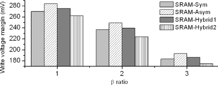
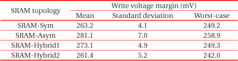
The write voltage margins of SRAM cells are evaluated in this section. The write voltage margin is measured as described in a previously published report [19]. The write voltage margins of SRAM cells are shown in Fig. 18. The asymmetrical pull-up transistor that is holding a “1” in SRAM-Asym produces lower contention current as compared to SRAM-Sym, SRAM-Hybrid1, and SRAM-Hybrid2. The write operations are thereby facilitated with SRAM-Asym. The write voltage margin of SRAM-Asym is by up to (depending on the β-ratio of SRAM cells) 10.6% wider as compared to the other SRAM cells that are investigated in this study. SRAM-Sym and the proposed hybrid asymmetrical SRAM cells (SRAM-Hybrid1 and SRAM-Hybrid2) have similar (difference less than 4.9%) write voltage margins.
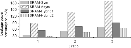
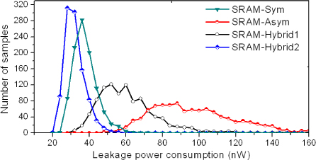
The leakage power consumed by different SRAM cells are compared in this section. The leakage currents are measured at 90℃ (assuming a short idle period near a hot spot [20]). The leakage power consumption of idle SRAM cells (bitlines are at 0.8 V and WL = 0 V) are shown in Fig. 19.
FinFET-Asym2 produces lower leakage currents as compared to FinFET-Sym and FinFET-Asym1 (as shown in Figs. 5 and 11). The second proposed hybrid memory cell SRAM-Hybrid2 therefore consumes the lowest leakage power among all the SRAM cells that are investigated in this paper. The leakage power consumption of the second proposed hybrid asymmetrical SRAM-Hybrid2 is reduced by up to (depending on the β-ratio of SRAM cells) 66.1%, 45.6%, and 15.5% as compared to the previously published purely asymmetrical SRAM-Asym, first proposed hybrid asymmetrical SRAM-Hybrid1, and symmetrical SRAM-Sym, respectively. The leakage power consumption of SRAM-Hybrid1 is up to (depending on the β-ratio of SRAM cells) 55.2% higher due to larger bitline leakage current as compared to the symmetrical SRAM-Sym.
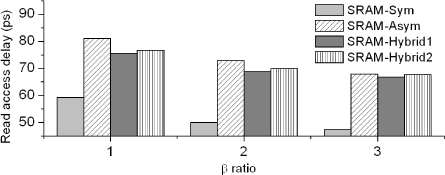
The worst-case (longest) read and write delays of the 128×64-bit memory arrays with different SRAM cells are compared in this section. The diffusion and gate capacitors of FinFETs are extracted from SRAM cell layouts using the Atlas device simulator [6]. Bitline and wordline parasitic impedances are extracted with Clever [6]. Π-type RC networks are used to characterize the worst-case (longest) data access delays.
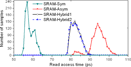
The read delay of an SRAM cell is the time interval from the 50% point of the WL low-to-high transition until a 200 mV voltage difference is developed between the bitlines. Due to stronger bitline access transistors, read data access with SRAM-Sym is up to (depending on the β-ratio of SRAM cells) 45.8%, 43.1%, and 41% faster as compared to SRAM-Asym, SRAM-Hybrid2, and SRAM-Hybrid1, respectively, as shown in Fig. 20.
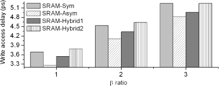
The write delay of an SRAM cell is the time interval from the 50% point of the WL low-to-high transition until one of the data storage nodes is charged from 0 V to Vdd/2. During write operations, the pull-up transistors in cross-coupled inverters of the purely asymmetrical SRAM-Asym produce the lowest contention current among the memory cells that are evaluated in this paper. The worst-case write operation with SRAM-Asym is therefore up to (depending on the β-ratio of SRAM cells) 16.1%, 13%, and 8.7% faster as compared to SRAM-Hybrid2, SRAM-Sym, and SRAM-Hybrid1, respectively, as shown in Fig. 21. The on-currents that are produced by the bitline access transistors in SRAM-Hybrid1 and SRAM-Hybrid2 during write operations are similar to SRAM-Sym. SRAM-Hybrid1, SRAM-Hybrid2, and SRAM-Sym therefore have similar write access delays (difference less than 5.4%).
4.7 SRAM electrical quality metric
The hybrid asymmetrical SRAM cells that are proposed in this paper are ranked differently for various important design metrics. A comprehensive SRAM Electrical Quality Metric is evaluated to identify the best memory circuit in this section. SRAM Electrical Quality Metric (SEQM) is
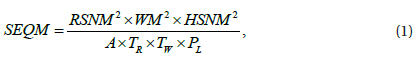
where A is the layout area of an SRAM cell. RSNM, HSNM, and WM are the read static noise margin, hold static noise margin, and write voltage margin, respectively, of an SRAM cell. TR and TW are the read and write delays, respectively, of an SRAM array. PL is the leakage power consumption of an SRAM cell. Degradation of data stability and write ability are important design concerns in nanoscale memory circuits. The read static noise margin, hold static noise margin, and write voltage margin are therefore emphasized by increasing the power of RSNM, HSNM, and WM terms to “2” in SEQM [28]. The silicon area, read delay, write delay, and leakage power consumption are assumed to be equally important for evaluating the overall electrical quality of a memory circuit.
The second proposed hybrid SRAM cell with asymmetrically gate-underlap engineered bitline access transistors (SRAM-Hybrid2) provides the highest read data stability and consumes the lowest leakage power. SRAM-Hybrid2 therefore provides the highest SEQM among all the SRAM cells that are evaluated in this paper. The overall quality is enhanced by up to (depending on the β-ratio of SRAM cells) 5.3 times, 2.5 times, and 57.7% with the proposed hybrid asymmetrical FinFET memory cell (SRAM-Hybrid2) as compared to SRAM-Asym, SRAM-Sym, and SRAM-Hybrid1, respectively.
5. CHARACTERIZATION WITH SIMILAR READ DATA STABILITY CONSTRAINT
The proposed hybrid asymmetrical SRAM cells provide stronger data stability as compared to the conventional symmetric and previously published purely asymmetric SRAM cells with minimum sized transistors. The conventional symmetric SRAM-Sym and previously published purely asymmetric SRAM-Asym [13] are re-sized to provide similar read data stability (within 1%) as compared to the proposed hybrid asymmetrical SRAM cells in this section. Multiple fin-heights FinFET technology [29] with maximum aspect ratio of 2.5 is assumed to size the SRAM cells. For providing equal read data stability at the nominal power supply voltage (Vdd = 0.8 V), the layout area of the symmetric SRAM-Sym and previously published purely asymmetric SRAM-Asym are increased by 8% as compared to the proposed hybrid asymmetrical SRAM cells. Impact of transistor sizing on leakage power consumption, active power consumption, write voltage margin, and hold data stability of all the SRAM cells that are investigated in this paper are listed in Table 1. Due to the increased β-ratio, the transition regions of the voltage transfer characteristics of cross-coupled inverters in SRAM-Sym and SRAM-Asym are moved away from Vdd/2. The hold data stability of the proposed hybrid asymmetrical SRAM cells are therefore 15% and 10.2% higher as compared to the purely asymmetric SRAM-Asym and symmetric SRAM-Sym, respectively, as listed in Table 1.
[Table 1.] SRAM circuits under similar read static noise margin constraint.

SRAM circuits under similar read static noise margin constraint.
Switching threshold voltage of cross-coupled inverters are reduced with increased β ratio. The proposed hybrid asymmetrical SRAM cells therefore provide up to 21.8% and 9.8% higher write voltage margins as compared to the symmetric SRAM-Sym and previously published purely asymmetrical SRAM-Asym, respectively, as listed in Table 1.
Bitline access transistors in SRAM-Sym, SRAM-Asym, and SRAM-Hybrid1 produce larger leakage currents as compared to SRAM-Hybrid2. SRAM-Asym, SRAM-Hybrid1, and SRAM-Sym therefore consume up to 3.94 times, 83.7%, and 68.9% higher leakage power, respectively, as compared to the proposed SRAM-Hybrid2. SRAM-Sym and SRAM-Asym consume slightly larger active power (difference less than 6.7%) as compared to the proposed hybrid asymmetric SRAM cells, as listed in Table 1.
6. IMPACT OF UNDERLAP (OVERLAP) LENGTHS VARIATIONS
The electrical characteristics of SRAM cells become increasingly sensitive to process parameter fluctuations with CMOS technology scaling [1]. Minimum sized (β = 1) SRAM cells tend to display the highest sensitivity to process parameter fluctuations [1]. Minimum sized SRAM-Sym, SRAM-Asym, SRAM-Hybrid1, and SRAM-Hybrid2 are therefore evaluated under gate-underlap (overlap) length variations in this section. 1000 Monte-Carlo simulations are run with Atlas. The left underlap (overlap) and right underlap lengths are assumed to have independent Gaussian distributions. The parameters of each transistor are varied independently. The underlap (overlap) lengths of FinFETs have 3σ variation of 2 nm. The statistical distributions of read access delay, leakage power consumption, write voltage margin, and read static noise margin (RSNM) of different SRAM cells are shown in Figs. 22, 23, 24, and 25, respectively.
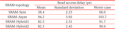
During read operations, the pull-down transistors in cross-coupled inverters of SRAM cells operate in linear region. Transistors with lower source/drain doping concentration are more sensitive to process parameter variations as compared to the transistors with higher diffusion doping concentration when the region of operation is linear [30]. For suppressing the susceptibility to process parameter variations during read operations, the diffusion regions of pull-down transistors in cross-coupled inverters are required to be heavily doped. A large portion of the right diffusion region of each pull-down transistor in cross-coupled inverters of the previously published purely asymmetric SRAM-Asym is undoped. The pull-down transistors in cross-coupled inverters of SRAM-Asym are therefore highly sensitive to process parameter fluctuations. Standard deviation of read access delay with the previously published purely asymmetrical SRAM-Asym [13] is 76.2%, 60.4%, and 56.6% higher as compared to SRAM-Sym, SRAM-Hybrid2, and SRAM-Hybrid1, respectively, as listed in Table 2. The mean of read access delay is increased by 61.3%, 41.2%, and 40.9% with SRAM-Asym, SRAM-Hybrid1, and SRAM-Hybrid2, respectively, due to weaker bitline access transistors as compared to SRAM-Sym. The worst-case read access delays with SRAM-Asym, SRAM-Hybrid1, and SRAM-Hybrid2 are increased by 57.1%, 39%, and 37.3%, respectively, as compared to SRAM-Sym, as listed in Table 2.
[Table 2.] Read access delay under process parameter fluctuations.

Read access delay under process parameter fluctuations.
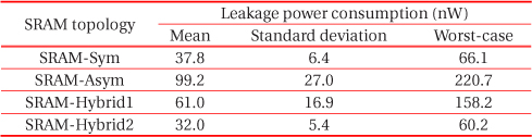
The asymmetrically gate overlapped / underlapped FinFETs (FinFET-Asym1) are more susceptible to process parameter variations during off-state as compared to the symmetrical FinFET-Sym and asymmetrical FinFET-Asym2. The previously published purely asymmetrical SRAM-Asym and first proposed hybrid asymmetrical SRAM-Hybrid1 therefore exhibit wider distributions of leakage power consumption as shown in Fig. 23. The standard deviation of leakage power consumptions with SRAM-Asym and SRAM-Hybrid1 are 4.2 times and 2.6 times larger, respectively, as compared to SRAM-Sym, as listed in Table 3. The standard deviation of leakage power consumption of SRAM-Hybrid2 is 15.4% lower as compared to SRAM-Sym. The mean of leakage power consumptions of SRAM-Asym, SRAM-Hybrid1, and SRAM-Sym are 3.1x, 90.4%, and 18.1% higher, respectively, as compared to SRAM-Hybrid2. The worst-case leakage power consumption of SRAM-Asym, SRAM-Hybrid1, and SRAM-Sym are 3.7x, 2.6x, and 9.7% higher, respectively, as compared to SRAM-Hybrid2, as listed in Table 3.
[Table 3.] Leakage power consumption under process parameter fluctuations.

Leakage power consumption under process parameter fluctuations.
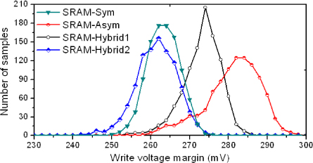
The pull-up transistors in SRAM-Asym produce lower contention current as compared to SRAM-Sym, SRAM-Hybrid1, and SRAM-Hybrid2. The mean of write voltage margin of SRAMAsym is therefore 7.5%, 6.8%, and 2.9% wider as compared to SRAM-Hybrid2, SRAM-Sym, and SRAM-Hybrid1, respectively, as listed in Table 4. The asymmetric pull-up transistors in cross-coupled inverters of SRAM-Asym are however highly vulnerable to process parameter variations. The purely asymmetric SRAM-Asym therefore has the widest distribution of write voltage margins, as shown in Fig. 24. The standard deviation of write voltage margin of SRAM-Asym is 70.7%, 42.9%, and 34.6% larger as compared to SRAM-Sym, SRAM-Hybrid1, and SRAM-Hybrid2, respectively.
[Table 4.] Write voltage margin under process parameter fluctuations.
Write voltage margin under process parameter fluctuations.
The distributions of read static voltage margins of SRAM cells are shown in Fig. 25. The bitline access transistors in the proposed hybrid SRAM cells are weaker during read operations as compared to SRAM-Sym. Furthermore, the pull-down transistors in cross-coupled inverters of the proposed hybrid SRAM cells are stronger as compared to SRAM-Asym. The mean of read static noise margin of SRAM-Hybrid2 is 90.7% and 58.5% higher as compared to SRAM-Sym and SRAM-Asym, respectively, as listed in Table 5. The means of read static noise margins of SRAM-Hybrid1 and SRAM-Hybrid2 are similar.
[Table 5.] Read static noise margin under process parameter fluctuations.
Read static noise margin under process parameter fluctuations.
Robustness of memory circuits against process parameter variations is determined by the “yield margin” (μ-6σ) test [7,24]. For a robust memory circuit, μ-6σ should be at least 4% of the power supply voltage. The yield margins of SRAM cells are listed in Table 5. μ/σ of SRAM-Sym, SRAM-Asym, SRAM-Hybrid1, and SRAM-Hybrid2 are 8.6, 5.6, 19.3, and 28, respectively. Due to smaller μ/σ, minimum sized symmetric SRAM-Sym and previously published purely asymmetrical SRAM-Asym are not stable under process parameter fluctuations. The second proposed hybrid asymmetric SRAM cell provides the highest robustness under process parameter fluctuations.
Two new hybrid six-FinFET SRAM cells with asymmetric bitline access transistors are proposed to enhance the read data stability and lower the leakage power consumption while maintaining a similar cell layout area and write ability as symmetric and previously published purely asymmetric SRAM cells. The strength of bitline access transistors is weakened during read operations and enhanced during write operations with the new hybrid asymmetric FinFET SRAM cells. The read data stability of the second proposed hybrid asymmetric SRAM cell (SRAM-Hybrid2) is enhanced by up to 71.6% and the leakage power consumption is lowered down to 33.9% while maintaining similar write voltage margin and identical cell layout area as other SRAM cells with 15 nm FinFET technology. Based on a comprehensive SRAM Electrical Quality Metric, the second proposed hybrid FinFET SRAM cell with asymmetrically gate-underlap engineered bitline access transistors (SRAM-Hybrid2) is identified as the most attractive circuit technique among the SRAM cells evaluated. SRAM-Hybrid2 enhances the overall quality by up to 5.3 times as compared to the other FinFET SRAM cells investigated in this paper. The effectiveness of the proposed hybrid SRAM cells are also verified under process parameter fluctuations.


![Purely asymmetric SRAM cell (SRAM-Asym) [13]. All of the six transistors are FinFETs with asymmetric gate overlap / underlap. Asymmetrically gate overlap / underlap engineered FinFETs are represented with shifted asymmetric thick lines along the channel. The transistor sizes (Width/Length) are in nanometers assuming a 15 nm FinFET technology.](http://oak.go.kr/repository/journal/20641/E1TEAO_2015_v16n6_293_f008.jpg)