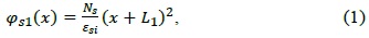
In recent times the tunneling field-effect transistor (TFET) has attracted a great deal of attention owing to its subthreshold slope (SS) < 60 mV/dec. As such, it is regarded as one of the potential replacements for conventional CMOS technology, which is facing many fundamental challenges in sustaining further technology scaling [1]. The operation principle of the TFET is based on band-to-band-tunneling (BTBT), which enables it to achieve a steeper SS. A TFET can be fabricated using existing semiconductor technologies, and for these reasons TFET is regarded as a very promising technology.
SPICE modeling has been the benchmark of logic- and circuit-level simulation and has played a vital part in the development of current CMOS devices. In order to investigate and better understand the performance of TFET-based logic devices and circuits, a fast compact model with medium accuracy needs to be developed. The literature in this regard is lacking. There are a few TFET Verilog models that exist [2-5]. However, [2,3] are lookup-table based models that require several fitting parameters; further, the fitting process in [2] is iterative. The model of [4] ignores the source and drain depletion lengths, which limits the accuracy of the model [6]. In the Verilog model of [5], the TFET drain current is found using a short-channel MOSFET model [7], which is physically incorrect for a TFET. Whereas [8] is a standard-reference TFET compact model, there is ambiguity in the use of tunneling parameters Ak and Bk used in the drain current expression of the model. The actual Ak and Bk values used in [8,9] are not clear. While a method to extract the Ak and Bk values from the data of drain current-gate voltage (Ids-Vgs) characteristics is presented in [10,11], the model of [10] and also [12] is for bulk TFET. Further, the model of [11] is piecewise with different equations for saturation and linear regimes of operation which is not suitable for SPICE modeling. Some other models [13,14] neglect the source depletion region, which at high Vgs becomes significant [6] and should not be ignored. Each of these issues restricts the accuracy of the existing models. In light of the above, there is a lack of a clear and accurate TFET compact modeling approach integrating all of the above-mentioned issues from a SPICE model point of view.
This lack of a concise modeling approach integrating all of the above mentioned issues impedes development of SPICE models for TFETs. In this work, we devise a clear double-gate (DG) TFET modeling approach and use it to develop a DGTFET Verilog-A model implemented in SPICE.
The paper is organized in the following sections. Section II explains the DGTFET compact modeling part. Section III includes the verification of the model. The conclusion is presented in Section IV.
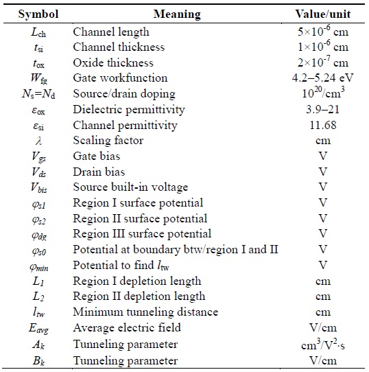
This section explains the DGTFET compact model. All the parameters used in the literature are mentioned in Table 1 given below.
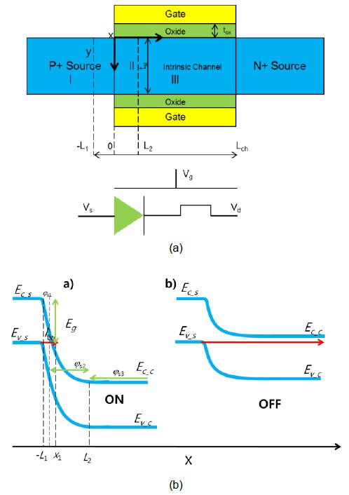
Fig. 1 shows the schematic of an N-type DGTFET (N-DGTFET). An N-DGTFET comprises a P+ source region with doping, an N+ drain region, and an intrinsic channel.
From a modeling point of view, a DGTFET is divided into 3 regions. Region I is composed of a source depletion region with L1 highlighting the length of the source depletion region as shown in Fig. 1. Region II comprises the tunneling junction between the source and channel with x=0 being at the boundary of both regions.
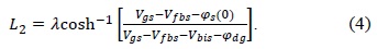
Here, L2 in region II specifies the length of the channel depletion region as indicated in Fig. 1(a). Region III comprises the transport region, where the charge carriers that tunnel through the tunneling barrier are transported to the drain by drift-diffusion with transport along the direction of the x-axis. Fig. 1(b) shows the band diagram of the DGTFET in on (left) and off (right) states.
A Poisson equation is solved in regions I and II with the help of boundary conditions to find the surface potentials in regions I and II. Following [15], the surface potentials φs1 and φs2 are given by
where Vfbs is the flatband voltage. The surface potential in region III, i.e. φdg, is calculated from [16] after making necessary adjustments for a DGTFET. The depletion lengths of regions I and II, i.e. L1 and L2, can be found by solving (1) and (2) together using their continuous potential and electric field at x=0. L1 and L2 are given by the following equations [15]:
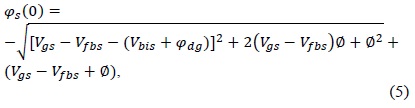
The potential at the internal boundary between region I and II is given by [15],
where is a constant in (5).
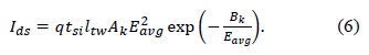
The drain current of the DGTFET can be given by the following expression obtained after making simplifying approximations [9,11,17].
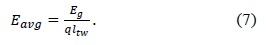
Here the average electric field is given by [8-14],
The minimum tunneling distance ltw could be described as the distance between the end of the source depletion region (i.e., region I) [8,10,11] and the point in region II where the surface potential has a value equal to the band-gap of the channel material. ltw can be given by [8],
In (8), φmin can be found by setting ∂ltw /∂φs2 = 0 [8,18] and is given by
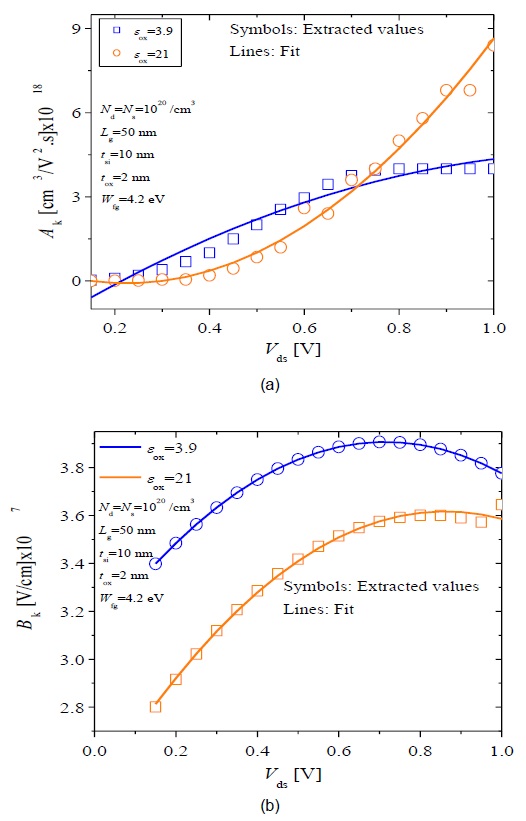
In (6), Ak and Bk are found [10,11] by taking the logarithm on both sides, such that it can be written as
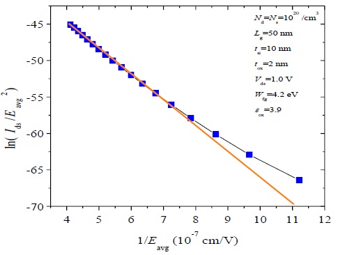
Ak and Bk can be extracted from (10), for a fixed Vds bias value as the intercept and slope of (10). Here Ids is obtained from the TCAD simulation results [19], and Eavg is calculated from (7).
The extraction procedure for a fixed Vds value is shown in Fig. 2, whereas extracted Ak and Bk values and their polynomial fits (lines) are shown in Fig. 3(a) and (b), respectively, as a function of Vds. Equations for second-order polynomial fits for Ak and Bk are given below.
where A0, A1, A2, B0, B1, and B2 are the fitted parameters.
Eqs. (11) and (12) were used to develop the SPICE model for the DGTFET, and are a very important component of the SPICE model. While only 2 dielectric constants were considered in this work, the procedure presented in this work is general and could be used to develop SPICE models for any combination of DGTFET device parameters mentioned in Table 1.
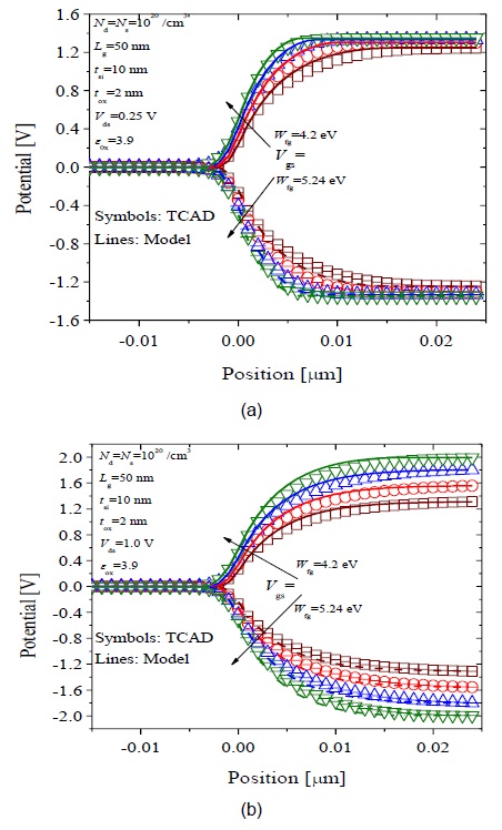
Two types of devices were considered in this section. Equivalent parameters (mentioned in Table 1) were considered for both the devices except for εox =3.9 with device 1 and εox =21 with device 2. N-type (N-DGTFET) and P-type (P-DGTFET) versions of both devices were considered in this work. For simplicity, the equivalent hole and electron tunneling mass was used for the P-DGTFET and N-DGTFET, respectively. In addition, the work function difference for both the P-DFTFET (Wfg =5.24 eV) and N-DGTFET (Wfg =4.20 eV) were adjusted in TCAD such that the Ids -Vgs characteristics obtained were equivalent. Fig. 4 shows the potential profile along the channel length for both N-type device 1 and P-type device 1 calculated from the model (lines) compared with the potential profile obtained from the simulator (symbols) for Vgs ranging from ±0.25 to ±1 V with increments of ±0.25 V and Vds held constant at Vds = ±0.25 V (Fig. 4(a)) and Vds = ±1.0 V (Fig. 4(b)). Here ‘+’ and ‘–’ indicate the bias for the N-DGTFET and P-DGTFET, respectively. The open symbols and solid lines indicate the potential for the N-DGTFET. The filled symbols and dashed lines indicate the potential for the P-DGTFET. The calculated potential profile is in good agreement with that obtained from the simulator.
The potential profile from Fig. 4(a) with Vds =±0.25 V clearly shows the surface potential increasing linearly with increasing Vgs and also becoming steeper. This increases the electric field at the source-channel junction resulting in reducing the minimum tunneling distance.
Fig. 4(b), which shows the potential profile for a higher Vds =±1.0 V, demonstrates that with increasing drain bias, the inversion electron concentration is reduced in the channel, allowing for effective unpinning of the channel fermi level.
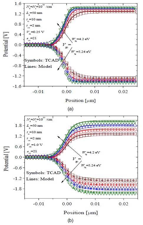
Fig. 5(a) and (b) show the potential profile for N-type (open symbols [TCAD], and solid lines [model]), and P-type (filled symbols [TCAD] and dashed lines [model]) device 2, which has a higher εox =21 at the same Vgs and Vds bias conditions as Fig. 4(a) and (b). Fig. 5(a) and (b) clearly show stronger saturation as compared to Fig. 4(a), and (b), respectively, and much shorter channel depletion lengths. This demonstrates that the gate field is stronger in the case of a higher εox. Overall, the model results compare very well with simulation results.
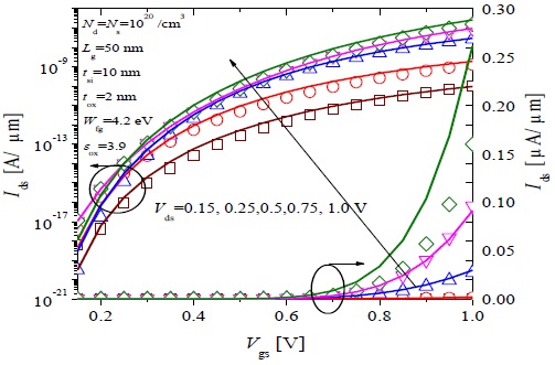
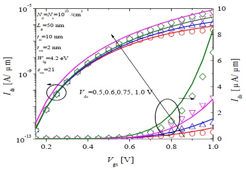
Figs. 6 and 7 show Ids -Vgs characteristics for N-type device 1 and P-type device 1, respectively, for a Vds ranging from ±0.15 to ±1.0 V. Here ‘+’ and ‘–’ indicate bias for the N-DGTFET and P-DGTFET, respectively. Both the model (lines) and simulation (symbols) show good agreement.
The parameters for Ak and Bk are fitted as A0 = -2.1195×10¹⁸, A1 = 1.0797×10¹⁹, A2 = -4.3336×10¹⁸, B0 = 2.4356×10⁷, B1 = 2.7468×10⁷, and B2 = -1.6002×10⁷ shown as blue lines in Fig. 3(a) and (b), respectively.
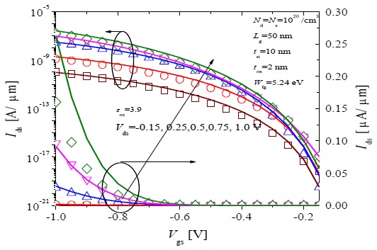
Fig. 8 shows Ids -Vgs characteristics for both N-type and P-type device 1, for Vgs values ranging from ±0.25 to ±1.0 V. Open (N-DGTFET) and filled symbols (P-DGTFET) indicate simulation results, and solid (N-DGTFET) and dashed lines (P-DGTFET) indicate results from the model. Reasonable agreement can be observed between the model and simulation results, particularly for high Vgs, which is a feature of Eavg -based models [9]. Here the same fitting parameters for Ak and Bk were used as those in Figs. 6 and 7.
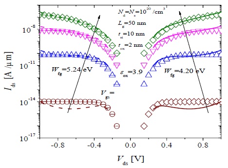
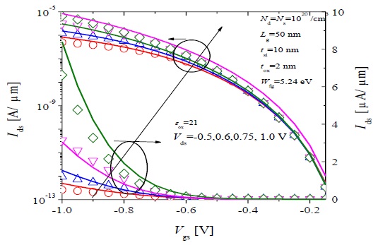
Figs. 9 and 10 show Ids -Vgs characteristics for N-type device 2 and for P-type device 2, respectively, calculated from the model (lines) using Ak and Bk with the parameters fitted as A0 = 3.8153×10¹⁹, A1 = -5.2005×10¹⁸, A2 = 1.3295×10¹⁹, B0 = 3.0917×10⁷, B1 = 2.2843×10⁷, and B2 = -1.597×10⁷ as shown by the orange lines in Fig. 3(a) and (b), respectively, with the simulation (symbols). The model captures very well the effect of varying device structural parameters on device characteristics. A much higher Ids is obtained for device 2, which in agreement with Fig. 5, demonstrating that due to a thinner effective oxide, the increased gate field across the tunneling junction results in increased current.
A SPICE model for a DGTFET is presented in this work. The method of Zhang et al. [8,15] was adopted to obtain the DGTFET surface potential, and the method developed by [4] was used to extract the Ak and Bk values for 1) a device with conventional SiO2 as a dielectric and 2) for a high-κ device with εox =21. The extracted Ak/Bk values were fitted using a second-degree polynomial. Using the fitting equations, a DGTFET SPICE model was developed. SPICE simulation results were presented for the DGTFET. By finding relevant Ak/Bk fits, the procedure presented in this work could be used to expand the current SPICE model to any combination of DGTFET structural parameters. Future expansion of the current SPICE model includes using constant Ak/Bk values as a function of Vds to achieve Ids -Vgs saturation in order to enable SPICE simulation for a wide range of logic devices including inverters. The SPICE model presented here does not need various fitting parameters, unlike [2,3], and is easy to use. The SPICE model compares very well with TCAD simulation results and offers a definite computational advantage over TCAD.