The frequency bands beyond 100 GHz can be utilized for various fields such as communications, imaging, radar, spectroscopy, and so forth. This frequency band is attractive from various aspects in comparison with lower frequency bands, including its wide bandwidth and high resolution for communication and imaging applications, respectively [1, 2]. For the implementation of high-frequency systems, a high-frequency signal source is an essential component because it plays a key role for transmitters as well as the local oscillators of receivers. Nevertheless, it is quite challenging to realize signal sources that operate beyond 100 GHz based on transistor technologies due to the limited operation speed of the transistors, especially when a considerable output power is desired. The challenge becomes more severe when signal source development is based on CMOS technology, which is predominantly used for modern electronics for its low cost, high reliability, and compatibility between analog and digital circuits. With the continuous advance of CMOS technologies, however, it has recently become feasible to develop signal sources that can operate beyond 100 GHz using CMOS technology. This study presents a 180-GHz signal source based on a 65-nm CMOS technology.
Several approaches can be applied to the design of signal sources that operate at high frequencies. The first approach is to use the fundamental-mode oscillator. However, designing fundamental-mode oscillators that operate near
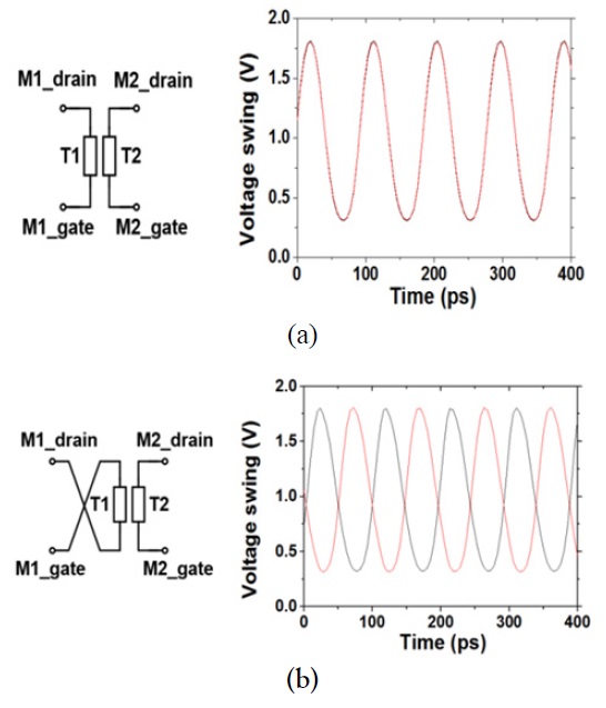
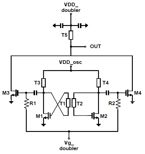
Fig. 1 is the schematic of the 180-GHz signal source developed in this work. The signal source consists of a 90-GHz differential oscillator and a 180-GHz frequency doubler. The 90-GHz fundamental-mode oscillator is designed based on Colpitts topology, which is preferred particularly for its high frequency operation compared to the LC cross-coupled topology, since it exhibits better phase-noise performance. On the other hand, Colpitts topology is naturally a single-ended structure and thus two Colpitts oscillators must be properly coupled together when a differential output is needed, which contrasts with the LC cross-coupled topology that inherently generates a differential output. As the frequency doubler employed in this work has a differential input, a coupling of two individual Colpitts oscillators is required to generate a differential oscillator output. Various coupling methods can be considered, but, ideally, the coupling should not significantly affect the resonance frequency of the individual oscillators. For this purpose, a coupled-line structure has been used in this study.
The coupled-line employed in this work is based on two transmission lines, T1 and T2, which provide the gate-drain feedback for M1 and M2, respectively. There are two options for the coupling of T1 and T2: forward (Fig. 2(a)) and reverse (Fig. 2(b)). With the forward coupling, the output voltage swings of the two oscillators are in-phase, as shown by the simulation in Fig. 2(a). On the other hand, with the reverse coupling, the two voltage swings show the opposite phase (Fig. 2(b)), leading to the desired differential output. Hence, the reverse coupling has been adopted in this work. The LC tank of the oscillator core, which determines the oscillation frequency, consists of T1 (and T2) and the parasitic capacitances CGS and CDB of M1 (and M2).
The output of the oscillator is directly connected to the input of the frequency doubler through a pair of DC block capacitors without a buffer in-between. The frequency doubler is based on a common-source differential pair, the output being taken at the common drain node. In the ideal case, only even harmonics will appear at the output node, but odd harmonics may show up if there is any mismatch in practical cases. To filter out the unwanted frequency components, including odd harmonics, a λ/4 short stub at 180-GHz is added at the output node of the frequency doubler.
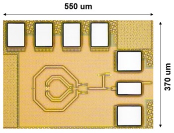
The 180-GHz signal source was fabricated based on Samsung 65-nm CMOS technology. The chip photo of the signal source is shown in Fig. 3. The total chip size, including RF and DC pads, is 370 × 550 μm2.
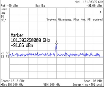
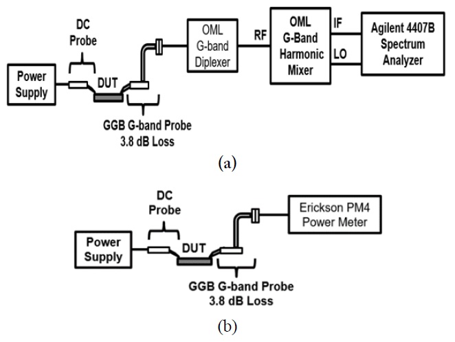
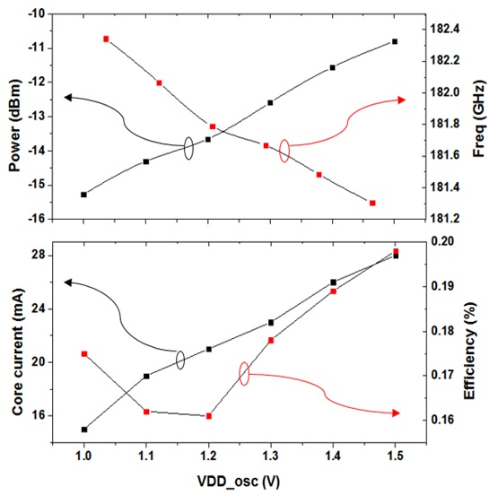
The fabricated signal source was measured for output spectrum with an Agilent E4407B spectrum analyzer using the setup described in Fig. 4(a). The measured spectrum is shown in Fig. 5, indicating an oscillation frequency of 181.3 GHz. The phase noise was estimated based on this spectrum profile, which was around -71 dBc/Hz at 1 MHz offset. The output power of the signal source was measured with an Erickson PM4 power meter with the setup shown in Fig. 4(b). The measured output power is plotted in Fig. 6 as a function of VDD_osc, together with the oscillation frequency. It is noted that VDD_osc serves as the drain as well as gate bias since the gate and drain of M1 (and M2) are shorted DC-wise. The output power varies from - 15.3 to -10.8 dBm, and the operation frequency varies from 181.3 to 182.3 GHz for the bias range of 1.0–1.5 V. The corresponding variations of the total current and the efficiency of the signal source are 15–28 mA and 0.17%–0.2%, respectively. Notably, the efficiency shows the highest value at the largest bias, indicating that the RF output power increases more rapidly with increasing bias than DC power dissipation does. The total power consumption of the signal source at the peak output power condition is 42 mW, the majority of which (33 mW) is from the 90-GHz oscillator.
A 180-GHz integrated signal source based on a 65-nm CMOS technology has been developed based on a 90-GHz oscillator and a frequency doubler. A coupled-line structure was successfully applied for the differential operation of the core oscillator.