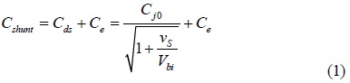
Power added efficiency (PAE) was used to validate the performance of the power amplifiers that are required to reduce power consumption with the purpose of maximizing the battery life and increasing the system performance. The switch-mode amplifier structure has been proposed to obtain a high efficiency; however, each class (class-D, -E, -F, and inverse class-F) of switch-mode power amplifiers (PA) has different advantages and disadvantages, which should be carefully considered. The class-D PAs are popular switch-mode PA for audio and RF frequencies; however, this class exhibits a poor efficiency at high frequencies because the parasitic reactance of the device leads to substantial energy loss. The class-F and inverse class-F PAs utilize a method that controls the harmonic components when the device operates in a saturation region to reduce overlapping between current and voltage waveforms, but the number of harmonics should be controlled to improve the efficiency. As a result, the harmonic that controls a circuit becomes complex and large. The switch-mode class-E PAs with a shunt capacitor produced by Sokal and Sokal [1] have an efficiency that theoretically reaches up to 100%. The operation of the linear shunt capacitance MOSFET class-E PA is completely different in a theory than it is in practical use. Because the parasitic drainto-source capacitance of the switching device, which significantly contributes to the overall shunt capacitance in the operation, is nonlinear, it is necessary to take into account the nonlinear characteristics of this capacitance. The analysis and design of a class-E PA with both a linear and nonlinear shunt capacitance, which was proposed by Suetsugu and Kazimierczuk [2], included figures and tables that contained the results of the numerical analysis of a design equation. These results were used to determine the values of the nonlinear shunt capacitance, the linear shunt capacitance, the series reactance of the resonant circuit, and the switch peak voltage; however, in some cases, it is impossible or inaccurate to calculate these parameters on the basis of the table and figures. The numerical analysis of the design equation determined by a program constructed in MATLAB is more exact than the value provided by the table and figures. For this work, the class-E power amplifier circuit was analyzed and designed by relying on the composition of the nonlinear and linear shunt capacitances to satisfy the zero-voltage switching (ZVS) and the zero-voltage-derivative switching (ZVDS) conditions, which ensure zero switching loss and low noise and improve component tolerances [3-5].
The role of a loaded quality factor of a series resonator module in class-E performance was also considered. A high value for the figure of merit is suitable for narrow bandwidth applications in which the harmonic content of the output is important. In contrast, low quality factor circuits are appropriate for applications in which the harmonic suppression of the output is not important. Typical applications include high-efficiency DC/DC converters; a radio-frequency energy supplies for heating, for the generation of plasmas, arcs, or sparks, and for communication jamming; or input drivers of a higher power stage [6]. In designing the class-E, the high quality factor of a resonant network has a limited frequency response. In some studies [7-9], the series LC resonator has been substituted by low pass or band pass matching networks to solve this limitation. Furthermore, the loaded quality factor of the resonant circuit has been reduced sufficiently to extend bandwidth operations and to reduce the sensitivity of amplifier performance to the values of resonator circuit elements [10]. A trade-off between bandwidth and the harmonic content of the output depending on the value of the quality factor is presented in this paper.
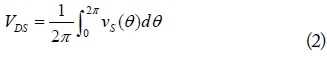
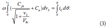
II. CURCUIT ANALYSIS AND PARAMETERS
Suetsugu and Kazimierczuk [2] presented a set of design equations for the class-E amplifier composed of both a nonlinear capacitance and a linear capacitance, which can be applied to real design; however, the results provided by the figures and tables in his paper are only considered in some discrete specifications. Therefore, instead of relying on his research results, the MATLAB program was built to solve design equations at our specifications. Furthermore, this study also illustrates the relationship between the frequency and the shunt capacitance in detail.
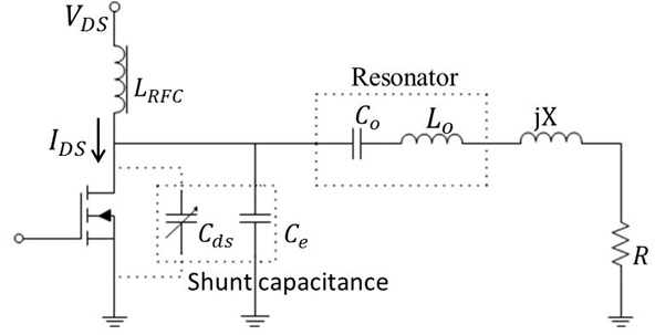
A circuit of the class-E amplifier is illustrated in Fig. 1, which shows a DC-supply voltage

where
The switch voltage is supposed to satisfy the ZVS condition at the turn-on time. Since the dc component of the voltage dropping across the choke inductor

where

By partly expanding Eq. (2):

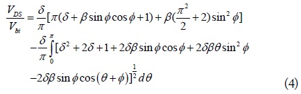
where


Because Eq. (4) does not have an analysis solution, a nonlinear function of the optimization toolbox of MATLAB was used to solve this equation. The key function of the MATLAB program used to solve a system of nonlinear equations is

where

where
Based on the analysis results, the schematic of the completed class-E PA circuit is modeled in Fig. 3. In this circuit, the output matching network is constructed by
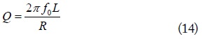
In the design of a broadband class-E PA with a shunt capacitance, the value of the optimal shunt capacitance changes at different frequencies, whereas the external capacitance is constant. Thus, an optimal state is impossible to obtain at every frequency. In this work, the value of the external capacitor was selected to approximately satisfy the switching conditions for the whole band.
III. BROADBAND CLASS-E PAS WITH A LOW Q RESONANCE
Some studies have investigated the role of quality factor

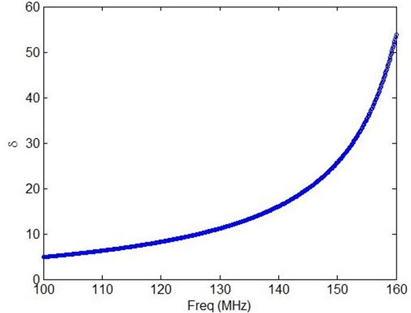
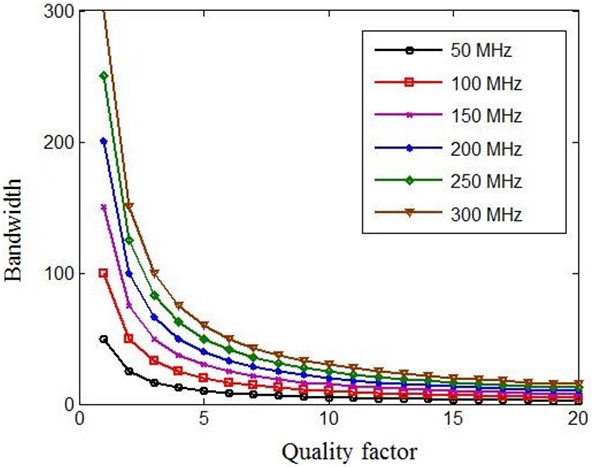
A high quality factor resonant circuit has a narrow bandwidth, which is different from a low quality factor. This relationship is expressed in detail in Fig. 5.
The nonlinear shunt capacitance class-E shown in the previous section was optimized for the narrow band design, as the loaded quality factor of the output resonant circuit is high enough that the output current would be considered a sine wave; however, because the loaded quality factor has finite and sufficiently small values with the assumption of harmonic distortion in the output signal, the efficiency increases by several percentage points [12]. As a result, the range of the value of the loaded quality factor is from 5 to 10 to obtain a high efficiency and a linearity at a single frequency [10].
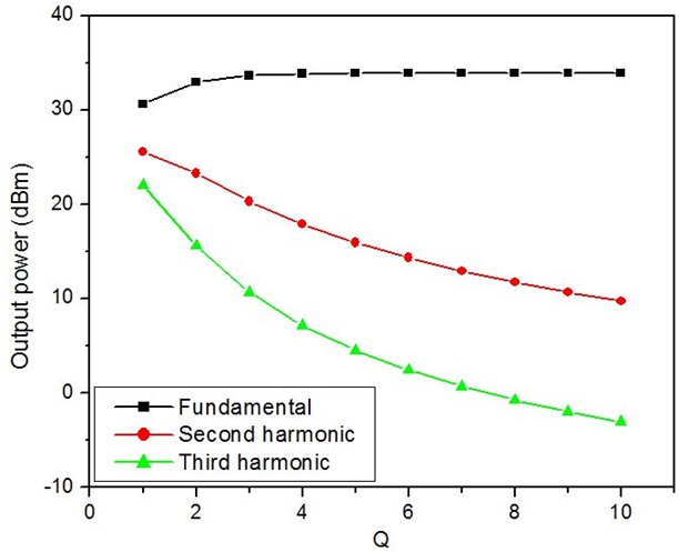
For this work, the operating bandwidth of the MOSFET class-E power amplifier was attempted to be extended by decreasing the value of the loaded quality factor to below the conventional values. In Fig. 6, the simulated output power sweep, containing fundamental, second, and third harmonics, is plotted as a function of the loaded quality factor. This result is based on the conditions of an operating frequency of 155 MHz, a supply voltage of 8 V, a MRF282SR1 MOSFET, an expected output power of 3 W (34.7 dBm), and without matching components. At different values of the low loaded quality factor, the components of the class-E power amplifier were approximately extracted from Eqs. (8)–(11). As a result, the fundamental output power cannot be achieved as expected at a low
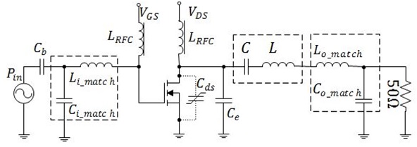
The topology of the class-E power amplifier for a wide bandwidth is similar to that of a single frequency as shown in Fig. 3; however, a wider bandwidth should be considered for quality factor of the input and output matching networks. A matching high-Q termination leads to narrow bandwidths.
IV. CIRCUIT DESIGN AND MEASUREMENT
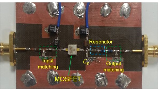
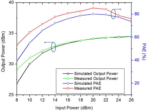
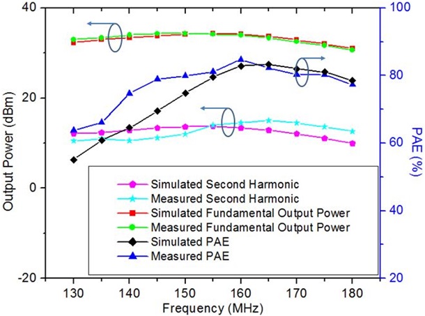
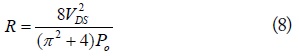
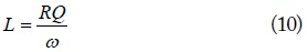
The proposed class-E power amplifier circuit was designed using a MRF282SR1 MOSFET transistor. The specifications of this design contain the output power of 3 W or 34.7 dBm and a bandwidth of 130 MHz to 180 MHz, which can be applied for Public and Homelands Security Applications [18]. Using Eq. (13), the value of the loaded quality factor is equal to 3.2. Based on the analysis in Section II, the calculations, simulations, and measurements of the component values were obtained and are shown in Table 1. The optimized values for accumulating the highest efficiency in the measurements caused the slight difference from the calculated component values. Fig. 7 presents a photograph of the prototype. The output power was measured using an Agilent 8565EC spectrum analyzer, which has a maximum measurement output of 30 dBm. An attenuator of -39.5 dB was added to the end of the circuit. The peak output power and PAE were achieved at 34.3 dBm and 84.8%, respectively, over a bandwidth from 130 MHz to 180 MHz. The drain and gate voltages were set to 8 V and 3.2 V, respectively. The power attenuation of the measured results occurred due to the relatively high harmonic output signal caused by the low loaded quality factor
where
[Table 1.] Component values of class-E circuit in calculation theory, simulation and measurement
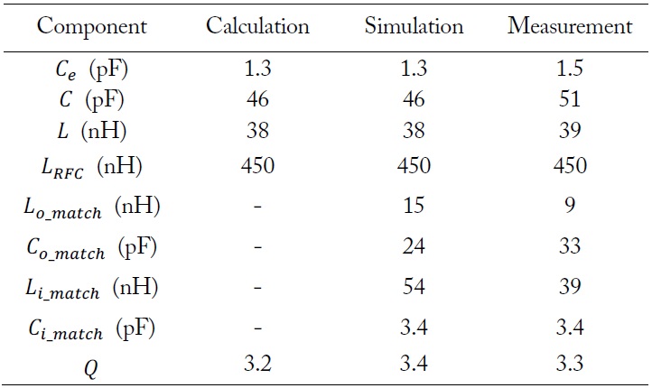
Component values of class-E circuit in calculation theory, simulation and measurement
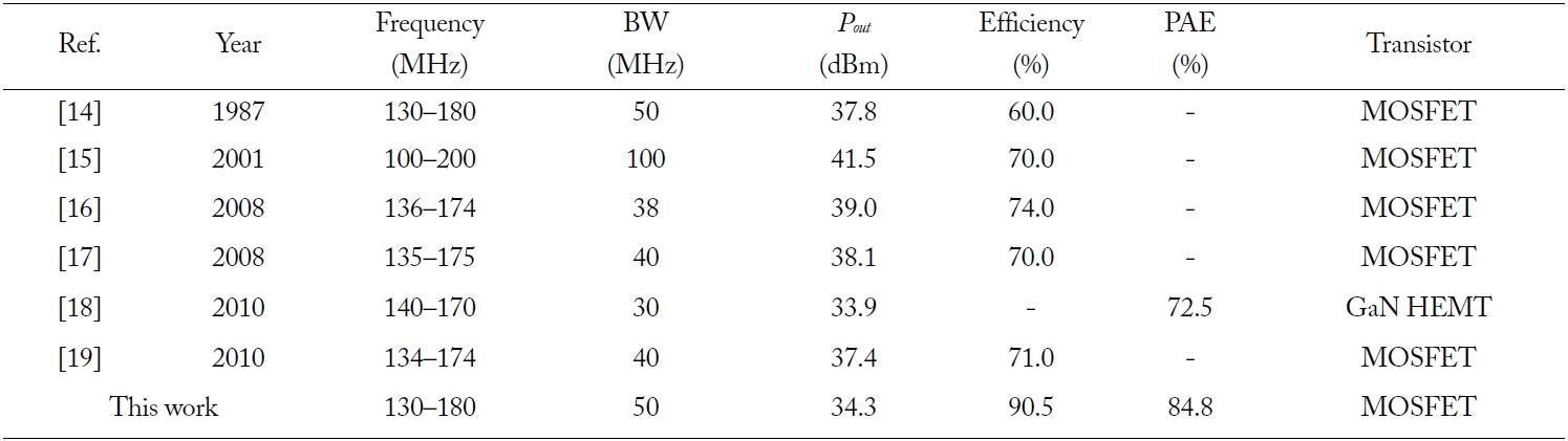
[Table 2.] Comparative results

Comparative results
This paper has presented a practical broadband class-E PA circuit which was designed using the combination of a nonlinear shunt capacitance and a low quality factor of series resonator. This method showed a high performance in designing broadband PAs for application at the VHF band. The validated design was developed using 130–180 MHz with a peak PAE of 84.8% and a peak output power of 34.3 dBm. Two outstanding advantages of the class-E PA with a shunt capacitance, which are a high efficiency and a simple topology, have been illustrated in this work.