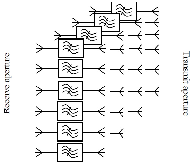
An antenna-filter-antenna (AFA) element is composed of a receive antenna, a non-radiating resonant structure, and a transmit antenna operating between the input and output radiation ports [1]. These elements can be used for designing transmitarrays (TA), when structured in a non-uniform array configuration [2]. They may also be used for designing frequency selective surfaces (FSS) when structured in a uniform array configuration [3]. The FSS can be viewed as filters with radiative ports, which are generally realized using planar periodic structures. Depending on the geometry, a single-layer FSS can present a bandpass or band-stop response around its resonant frequency.
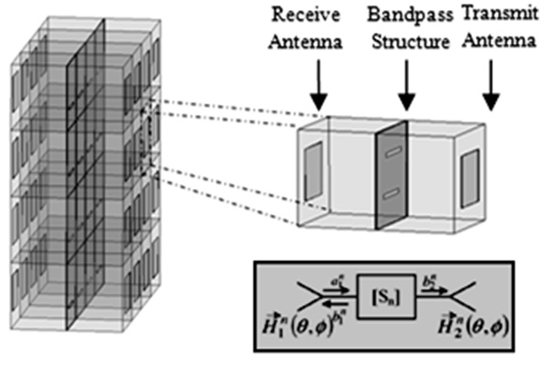
In general, these elements are formed as three layer metallic structures: two resonant type planar antennas in the top and bottom layers, and one or more planar transmission line or slot resonators in the middle layer. Using AFA elements in the transmit-arrays results in a bandpass transfer function whose characteristics are desirable for radar, satellite [4], and power combining applications [5], where the distributed nature of the transmit-arrays can improve the power-handling and heat dissipation in the structure.
High-order filters are commonly designed using multi-layer FSS structures [6, 7]. Since the computational complexity drastically increases for multiple layers, the design of high-order frequency selective surfaces is performed by combining the individually designed FSS layers. The FSS layers, acting as individual resonators, are stacked using thick (0.2–0.3
This paper introduces a new approach to the AFA element design as a simple three-layer structure consisting of two patch antennas and co-planar waveguide (CPW) resonators. In contrast to the conventional stacked FSS designs, a higher order response can be achieved by simply adding resonators in the CPW layer, instead of increasing the number of layers, which simplifies the design significantly. The paper also demonstrates the measurement method used to extract the focusing
The rest of the paper is organized as follows. In Sections II and III, we introduce the concept and design of the AFA element. The measurement method and the characterization of the proposed elementary cell are discussed in Section IV. Finally, conclusions are drawn in Section V.
II. AFA CONCEPT & CIRCUIT MODEL
1. Antenna-Filter-Antenna Concept
A schematic representation of an AFA array is shown in Fig. 1. Each AFA module is composed of receive antenna, a nonradiating resonant structure, and a transmit antenna [8-12]. Although the frequency characteristics of the antenna set the limit on the transmission bandwidth of these modules, a more general category of filtering shapes can be synthesized using this method. A simple example of such an FSS has been proposed in [6] (based on an earlier work [13]), where a pseudo-highpass filter is formed between the input and output apertures of an array of open ended waveguides.
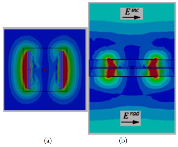
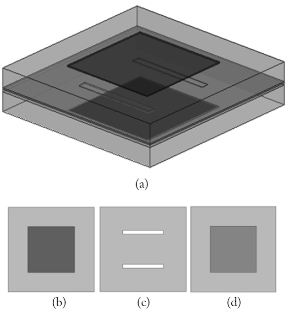
Fig. 2 shows a case where the radiative elements in the AFA are two back-to-back microstrip patch antennas. The middle resonant structure is an ensemble of CPW resonators fabricated in the common ground plane (referred to as the CPW layer). The coupling between the antennas and the CPW resonators is achieved through coupling slots in the CPW layer. Use of the resonant-type radiative elements is advantageous, since a resonant element by itself can be considered as a combination of a radiative resistance and a resonator. The built-in resonators of the receive/transmit antennas can then be combined with the CPW resonant structure to form a bandpass filter between the radiative ends (see Fig. 3).
For a given filter order, this reduces the required number of the CPW resonators. Special case of the structure is used in [14], where two patch antennas are coupled through a non-resonant slot to form a two-pole bandpass filter. As opposed to the conventional stacked FSS design, a higher order response can be obtained simply by adding resonators in the CPW layer, instead of increasing the number of layers.
2. Antenna-Filter-Antenna Circuit Model
This section describes the general considerations in design of the radiative elements and coupling slots.
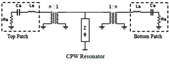
The circuit model of the elementary cell is illustrated in Fig. 3. It can be recognized as a band-pass filter. Around the resonant frequency, the antennas are seen as series RLC circuit from the point of view of the resonator. Resistance
The parameters in the antenna circuit model can be extracted from the simulation of the antenna and the coupling slot in an infinite structure, or in a periodic array with a cell size of 3.6 mm which is determined from the effective radiative aperture of the antennas [15]. The critical design parameter, after fixing the antenna and the slot line dimensions, is the value of coupling between the antennas and the resonator. This is controlled by the position of the coupling slot relative to the center of the patch. The proposed circuit model is only valid for a normal incident wave with the electric field polarized parallel to the slot resonator.
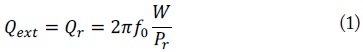
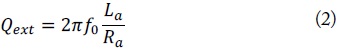
According to the circuit model shown in Fig. 3, the input/output coupling of the unit cell is related to the external
where

where
All components of this model are calculated using analytical expressions taking into account the physical parameters of the structure [2].
The elementary cell, illustrated in Fig. 4, consists of a single ground plane, two substrate layers (Rogers RT/duroid 5880,
The linear line slot in the ground plane is designed for a good matching for 42 GHz, which corresponds to wavelength in the substrate
Design and optimization of the element is relatively straightforward and converges after a handful of iterations, by handwaving between circuit and finite-elements models.
The elementary cell was designed with ANSYS-HFSS electromagnetic simulation software using Floquet ports and periodic boundary conditions.
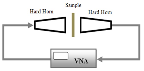
To provide an adequate characterization of the proposed cell we adopted a modified version of the Gaussian quasi-optical measurement systems GOMS [18].
GOMS uses a free space measurement setup that simulates the guided system. Quasi-optical measurement systems have been used for this purpose by a number of researchers [18] for performing similar measurements at 60–300 GHz. However, the required lens/mirror size and focal length prove impractical at Q-band.
Based on the hard-horn developed by Ali et al. [19], a guided measurement system can be developed to simulate an oversized parallel-plate waveguide. Hard-horns are antennas with nearly uniform aperture distribution, which are formed by dielectric loading of the metallic pyramidal horns. A specially designed dielectric lens is used at the aperture to compensate the spherical phase error across the aperture. The hard-horns act as a matched transition between the coaxial terminals and the oversized TEM waveguide ports. The sample under test can be sandwiched between two of these waveguide ports, to form a guided system with coaxial ports.
This system has been successfully used for excitation and measurement of Ka-band quasi-optical amplifier arrays [20]. In our application it is impractical to sandwich the FSS sample between the two hard-horns due to the loading effect of the dielectric lenses. Yet, the hard-horns can be used to form a quasi-guided system.
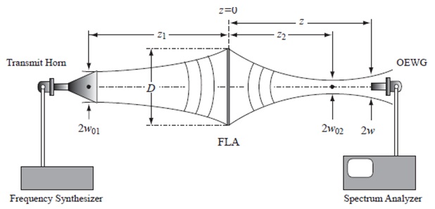
Fig. 6 shows an antenna array (FLA) in a Gaussian optics measurement system. An input axial beam of the waist radius
In our modified system, which is shown in Fig. 7, the hard horns form two parallel TEM ports that are separated by an air gap, and the sample under test is placed in the middle of two ports. Due to their high directivity, the hard-horns are expected to generate a good approximation of the plane wave in the nearfield, as is required for the FSS/TA measurements. As the sample can be freely reoriented in the air gap, the quasi-guided system proves convenient for performing measurements at arbitrary angles of the incidence. However, the oblique incidence measurement generally requires larger samples and a wider air gap.
Since the electromagnetic field in the gap region is assumed to be predominantly TEM, the air gaps between the hard horn apertures and the surface of the sample can be treated as transmission-line sections. This allows for a standard thru-reflect-line (TRL) calibration of the measurement setup, which simultaneously de-embeds the connecting cables, hard-horns, and air gaps, from the measurement [22]. Also a time-gating process is applied to filter out the residual error due to the multiple reflections of the high-order modes.
The measurement setup is based on Agilent 8510C vector network analyzer and the hard horns. The hard horns are used as transitions between coaxial input/output and planar wave fronts. A TRL calibration is applied to eliminate the effects of cables, connectors, hard horns, and the air gap between the hard horn apertures and the FSS samples.
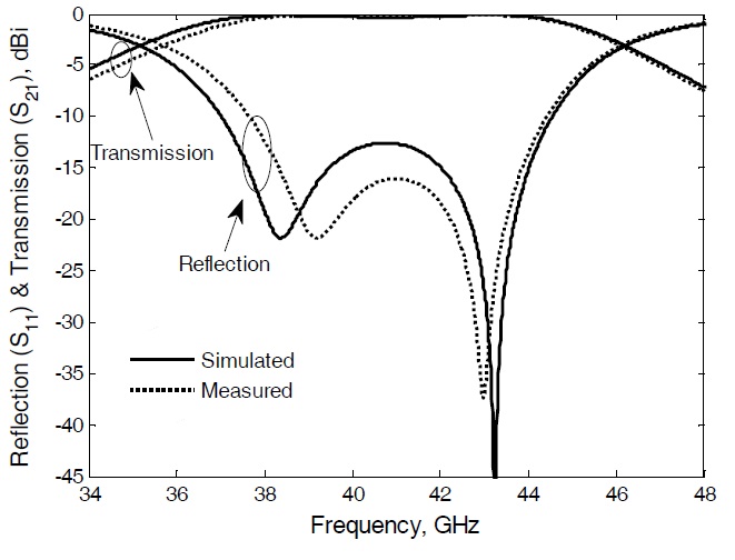
The simulated and measured
The maximum in-band insertion loss for this design is <0.2 dB.
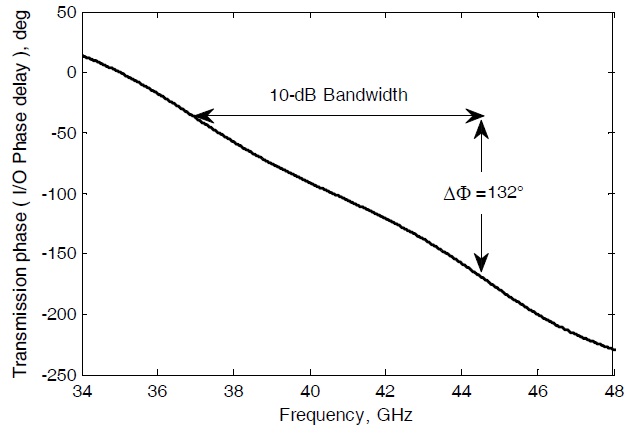
Fig. 9 shows the variation in the transmission phase of the AFA element. The phase difference in the 10-dB bandwidth is 132°.
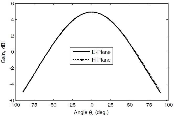
Fig. 10 depicts the computed radiation pattern of the AFA element at 42 GHz. It shows a maximum gain of 4.9 dBi and a 3-dB beamwidth of 86° in E-plane.
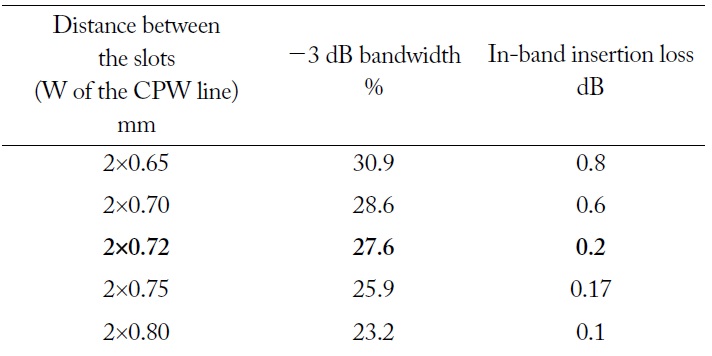
The coupling determines the filter’s bandwidth and in-band ripple, and can be controlled by changing the exposed distance between the two slots in the ground (W). Table 1 summarizes the matching performance.
[Table 1.] Matching performance of the elementary cell computed at 42 GHz

Matching performance of the elementary cell computed at 42 GHz
The designed unit cell is the first step of a future unit cell design for transmit-arrays. In the case of transmit-array, the main design challenge is the ability to generate the appropriate phase-shift for each cell in order to transform the incoming spherical wave on the free-space side (i.e. to produce a nearlyflat phase distribution or a given phase gradient depending on the main beam direction). Since this phase compensation cannot be ideal, we have previously investigated the effect of phase quantization on the directivity and gain of an array designed in X-band [4]. We have shown that a 1-bit (180° phase steps) and 2-bit (90° phase steps) design result in 4.3 dB and 0.8 dB loss, respectively, compared to the ideal case (Table 2).
[Table 2.] Impact of the phase quantization, transmit-array in X-band [4]
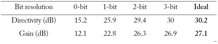
Impact of the phase quantization, transmit-array in X-band [4]
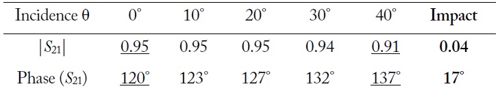
The effect of the skew incidence on the transmission performances of the proposed elementary cell has been investigated, and was found rather negligible (Table 3). It is worth mentioning that this impact can also be neglected in the case of transmit-array with phase quantization up to 3-bit; as the phase error in that case would be ± 22.5° which is larger than the maximum impact of 17° shown in Table 3.
[Table 3.] Impact of the skew incidence

Impact of the skew incidence
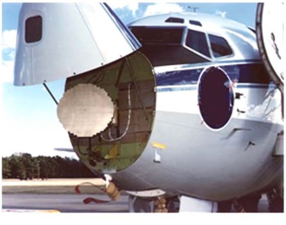
The designed AFA element (FSS) and the future detuned cell (TA) can be used together in the same application; FSS for radome and TA for radar antenna, as illustrated in Fig. 11.
A simply-structured wideband AFA element has been designed using patch antennas and CPW resonator. A uniform array of these elements exhibits a low loss and sharp roll-off frequency response, which makes it an excellent candidate for filtering application in quasi-optical amplifier arrays and grid mixers. This AFA element has been adequately characterized in non-anechoic environments by using a modified Gaussian optics measurement system. Attractive features, in terms of bandwidth and efficiency, have been achieved by the proposed design. The designed unit cell is the first step of a future unit cell design for lens-arrays and beam-steering for high-speed wireless communication.


![Antenna under test (FLA) in a Gaussian optics measurement system [21].](http://oak.go.kr/repository/journal/20370/E1ELAT_2015_v15n4_206_f006.jpg)


![Impact of the phase quantization, transmit-array in X-band [4]](http://oak.go.kr/repository/journal/20370/E1ELAT_2015_v15n4_206_t002.jpg)