The rapidly increasing demand for high-speed communication has spurred the development of new information and communication technologies aimed at satisfying growing highspeed needs. Numerous research groups are now actively reporting promising results for enhancements in high-speed wireless communications [1]. This technical trend supports the prediction that applications for frequency ranges beyond 100 GHz will be in the spotlight in the not so distant future. This frequency band has many advantages, such as wide bandwidth and compact size, which arise from its high frequency and small wavelength, respectively.
One of the key blocks in the high frequency wireless communication systems is the transmitter, which generally lacks sufficient output power at the high operation frequency. The currently available transistors are limited in their
This work introduces a D-band integrated signal source, which consists of a V-band oscillator, a V-band amplifier, and a D-band frequency doubler based on a SiGe BiCMOS technology.
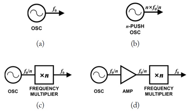
Several different methods are available for the design of a signal source that operates at high frequencies, as shown in Fig. 1. The simplest method is to use a fundamental-mode oscillator as a source, as shown in Fig. 1(a). However, designing a fundamental-mode oscillator that operates near
It is reported that a fundamental-mode oscillator integrated with a
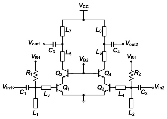
Fig. 2 shows the schematic of the V-band fundamental-mode oscillator developed in this work. The oscillator adopts the Colpitts topology, which is favored over the
Generally, the output power of an oscillator will increase with the size of the transistors, but the oscillation frequency will decrease. In this work, large size transistors were adopted in favor of the stable oscillation, given the rather sufficient margin for frequency budget. All sizes of the transistors
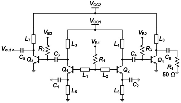
The output power of a source composed of an oscillator and a frequency multiplier can be boosted by adding an amplifier, either after the oscillator or after the frequency multiplier. The latter is more challenging because of the difficulty in achieving sufficient gain at higher frequency, due to the limitations in
The transistors
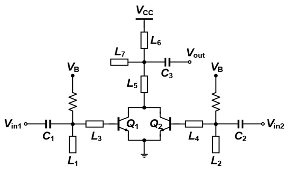
The schematic of the frequency doubler is shown in Fig. 4. It is based on a common-emitter differential pair, the output being taken at the collector common node. At this node, all the odd harmonics, which have opposite phases for the left and right branches of the pair, are canceled out. On the other hand, the even harmonics have the same phases at the two branches and they are added at this common node. Hence, only the even harmonics will appear at this node, with the second harmonic being the strongest in its signal power level.
The emitter lengths of
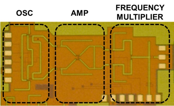
The D-band integrated signal source, combining the three circuits described above, was fabricated based on TowerJazz 0.18-μm BiCMOS technology. Individual circuits of each block were also fabricated for characterization of the individual circuit performance. A photograph of the integrated source is shown in Fig. 5. The total chip size, including RF and DC pads, is 900 × 1,890 μm2.
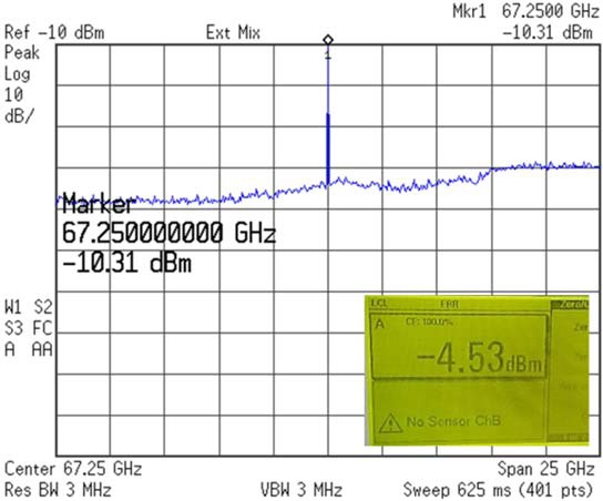
The fabricated individual oscillator was measured with an Agilent E4407B spectrum analyzer and Agilent E4419B power meter. Fig. 6 shows the measured spectrum, indicating an oscillation frequency of 67.3 GHz. The inset shows the measured output power, which is –4.5 dBm before loss calibration, which corresponds to a calibrated power of 2.7 dBm after loss compensation. The DC power consumption is 145 mW, leading to a DC-to-RF efficiency of 1.3%.
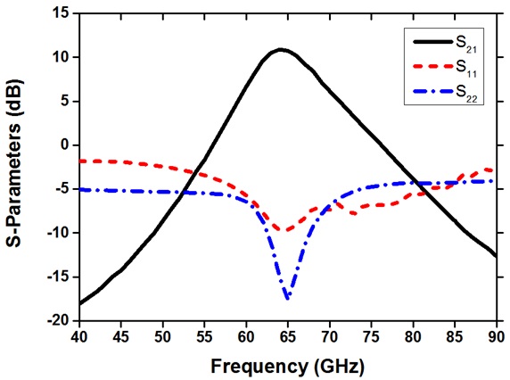
The small signal characteristics of the V-band amplifier were measured using an Agilent E8361A network analyzer through
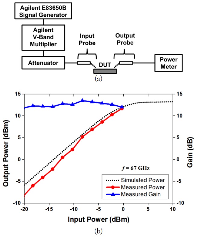
The amplifier was also characterized for the linearity, using the measurement setup shown in Fig. 8(a). The signal from a V-band source module powered by an Agilent E83650B signal generator was injected into the amplifier, and the output was determined by an Agilent E4419B power meter. An additional QuinStar QDA-V0000 attenuator was attached to the source module for input power control.
The measured linearity is shown in Fig. 8(b). Due to the limitations of the output power of the source module, measurements were only made up to an input power of around 0 dBm. However, a comparison with a simulation, which is also shown in the plot, indicates that the saturation power of the amplifier is expected to reach around 13 dBm. Together with the output power of the oscillator, 2.7 dBm, the output from the amplifier should be sufficient to drive the following frequency doubler.
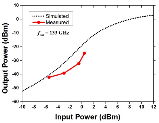
The measurement setup of the frequency doubler is identical to that for the amplifier linearity measurement, except that an Erickson PM4 power meter was used for the D-band power measurement. As already mentioned, due to the limited output power of the signal source, the measurements were made only up to an input power of around 0 dBm. The lower limit was also imposed by the noise floor level of the measurement (around –40 dBm), resulting in a few data points available from the measurement as shown in Fig. 9. However, the measurement shows a reasonably good agreement with the simulation for the measured range, as shown in the plot. Thus, the circuit is expected to follow the performance predicted by the simulation. This was actually verified with measurements of the integrated source, as described later. This circuit consumes 60 mW of DC power.
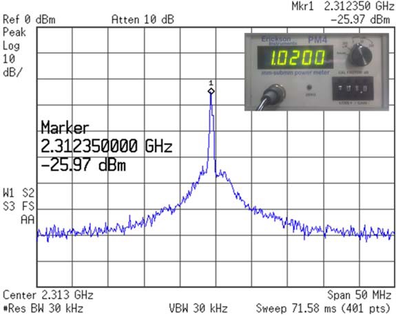
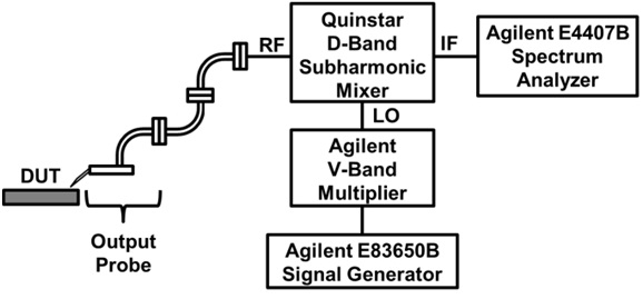
Finally, the integrated source was characterized using the setup shown in Fig. 10, which is composed of an Agilent E-4407B spectrum analyzer and a D-band external sub-harmonic mixer (2nd order) driven by a V-band source with an Agilent E83650B signal generator. The output spectrum of the signal source, with the frequency down-converted for testing, is shown in Fig. 11. The measured 2.31 GHz indicates that the output frequency of the integrated source is 133.2 GHz, considering the LO input (2
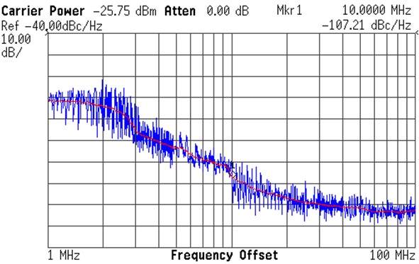
The inset in Fig. 11 shows the output power measured through an Erickson PM4 power meter (before calibration). With the loss of the D-band probe, known to be 3 dB, the calibrated output power is 3.1 dBm. The phase noise was measured as –107.2 dBc/Hz at a 10 MHz offset, as shown in Fig. 12. The total DC power consumption was 315 mW, leading to a DC-to-RF efficiency of 1.0%. The measured performance of the fabricated integrated source is compared with other signal sources operating around D-band in Table 1. This comparison indicates that the source developed in this work is among the best in terms of its output power level in this frequency range.
[Table 1.] Signal sources operating beyond 100 GHz based on Si-based technologies
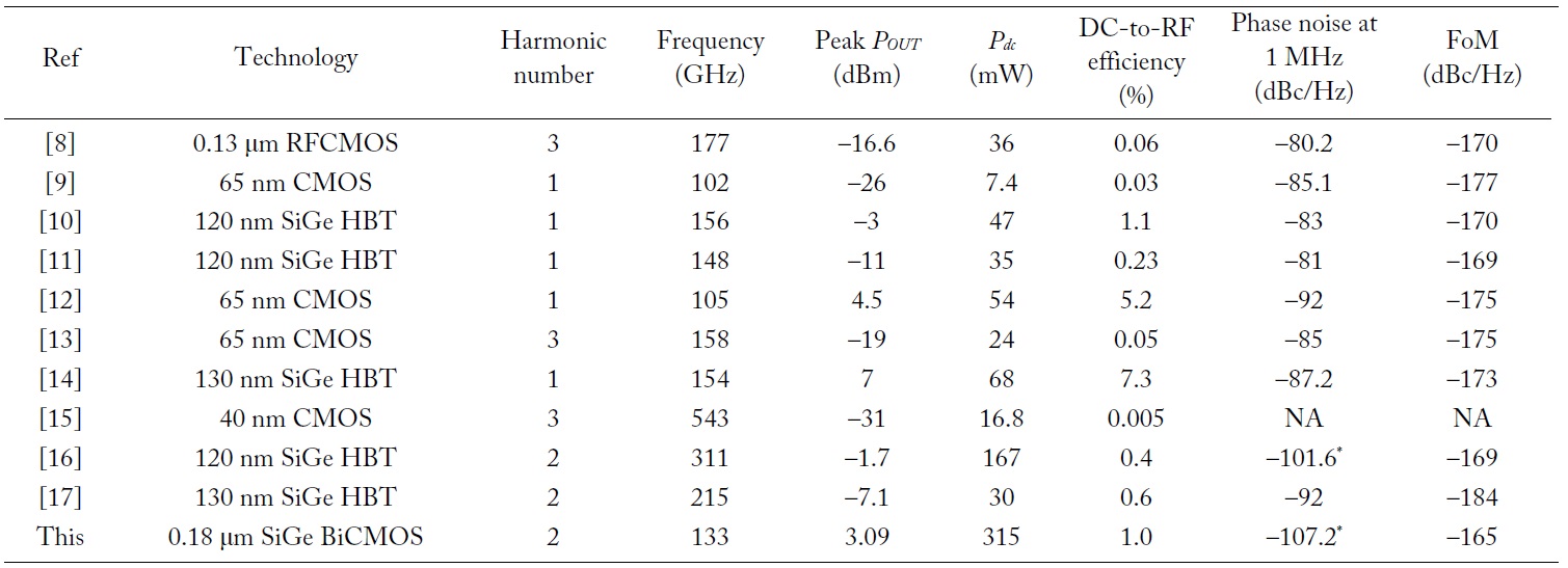
Signal sources operating beyond 100 GHz based on Si-based technologies
A D-band signal source based on a 0.18-μm SiGe BiCMOS technology was developed by integrating a V-band oscillator, a V-band amplifier, and a D-band frequency multiplier. The integrated source exhibited an output power of 3.1 dBm at 133.2 GHz and the phase noise was - 107.2 dBc/Hz at 10 MHz offset. The performances of the individual circuit blocks were also characterized. The employed topology for a signal source may represent an efficient solution for D-band high power signal generation.