Solar thermal selective coatings play a pivotal role in the construction and working of solar power systems. Solar selective absorber coatings are characterized by two important features: i) a very high absorptance and ii) a low reflectance in the solar spectral range of 0.3~2.5 μm [1]. A solar thermal selective absorber can convert solar energy of low density to heat energy of high density, improving the efficiency of a photo-thermal conversion [2]. In general, solar selective absorber coatings can be generally categorized into six components [3]: a) intrinsic absorber, b) semiconductor metal tandem, c) multi-layer absorber, d) multi dielectric composite, e) textured surfaces, and f) selective solar transmitting coating. An intrinsic absorber uses a material, having intrinsic properties and a requisite spectral sensitivity. The semiconductor-metal tandems absorb radiation of short wavelength, because of the semiconductor bandgap and a low thermal emittance. Multi-layer absorbers exhibit multiple reflection effect between multi layers in order to absorb solar energy. The metal dielectric composites are composed of fine metal particles, which are found in either the dielectric or ceramic host material. The textured surfaces exhibit high solar absorptance as multiple reflections occur on their needle-like or porous microstructure. Finally, the selective solar transmitting coatings are applied on an absorber that resembles a blackbody. Thus, such an absorber is functional even at low temperatures. Using these coating methods, we develop multi-layer absorber coatings with high absorption and low thermal emittance in the solar region. Therefore, they are stable at an elevated temperature, depending on the materials used in construction. A typical double-cermet layer of a film extends from the surface to a substrate, depicting a figure described as follows: an anti-reflection layer enhances solar absorption; an absorbing layer is composed of two homogenous cermet layers: a low-metal-volume fraction (LMVF) cermet layer on high-metal-volume fraction (HMVF) cermet layer; and a metallic infrared reflector layer that reduce emittance from the substrate [4-6].
Several multi-layer absorbers, consisting of different metals (Mo, Ag, Ni, Cr, and Ti) and dielectric layers (Al2O3, SiO2, CeO2, NiO, and Cr2O3), have been used as solar materials [7-10]. Recently, a coating made from either transition metal nitride or oxynitrides has attracted the attention of several researchers, because the constituents of the coating have remarkable chemical, mechanical, electrical, and optical properties. Furthermore, it has been reported that TiN, TiAlN, and TiAlNO have high absorption and low emittance in the deep infrared region [11]. Cubic CrN has a similar crystal structure containing TiN, and it shows excellent electrical conductivity, high oxidation resistance, and thermal stability. It is a well-known fact that CrN and AlCrN films have been widely used as protective coatings, because they possess chemical inertness and good thermal stability [12].
A variety of techniques, such as electro-deposition, CVD, evaporation, ion plating, pulsed laser deposition, and magnetron sputtering, can produce multi-layer cermet coatings [13-17]. With the help of magnetron sputtering, we can possibly apply on a large area deposition of thin films. Therefore, they are highly suitable for use as solar selective absorbers or multi-layer films without contamination. However, presently, very few reports have described about the optical and surface properties of AlCrNO and TiNO multi-layer films. In this study, we prepared multi-layer AlCrNO and TiNO cermet films on Al substrate by conducting a dc reactive magnetron sputtering method. Thereafter, their optical properties and microstructure were investigated on the basis of a change in the rates of gas mixtures.
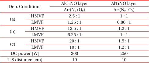
A dc magnetron sputtering system was used for applying a solar selective multi-layer coating. This sputtering system was of the sputter-down category. At a purity level of 99.995%, the Al:Cr(5 wt.%) and Al:Ti(10 wt.%) target was sputtered in a mixture of gases: Ar(99.99%), N2(99.99%), and O2(99.995%); these gases constituted the sputtering atmosphere. The 5-layer thin film solar selective absorbing deposition was executed subsequently on an Al substrate. An antireflection layer of Al2O3 was prepared at a pressure of 20 mTorr, which was exerted by a mixture of Ar and O2 gases. In cermet films, the volume fraction of the metal component was controlled by the mixing rates of Ar:(N2+O2) gas . The sputtering parameters are enlisted in Table 1.
[Table 1.] Sputtering conditions of multi-layer solar absorber films.
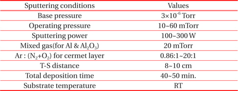
Sputtering conditions of multi-layer solar absorber films.
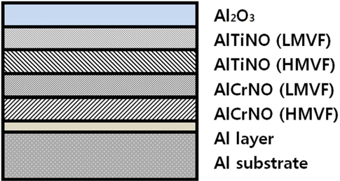
Figure 1 presents a schematic structure of Al2O3/AlTiNO/AlCrNO/Al multi-layer cermet absorber. An Al metal acts as an infrared reflecting layer on the substrate, reducing the emittance of the substrate. The absorbing multi-layer film consists of two AlTiNO and AlCrNO cermet layers, with different volume fractions of metals. As shown in Fig. 1, in the layer (third cermet layer) near the substrate, there is a high metal volume fraction (HMVF) of AlCrNO. In the next layer, there is a low metal volume fraction (LMVF). Subsequently, HMVF layer of AlTiNO is located on the AlCrNO cermet layer, while LMVF of AlTiNO layer is positioned near the antireflection layer. The top antireflection layer is a transparent Al2O3, which ensures higher solar absorption.
The surface micrograph of a multi-layer thin film was estimated by field emission scanning electron microscophy (FE-SEM). The exact composition and optical properties of cermet absorber films were measured by Auger electron spectroscopy (AES) and UV-Vis-NIR spectroscopy, respectively. The reflectance of absorber thin films were measured in the wavelength ranges of 0.3~2.5 μm using UH4150 UV-Vis-NIR spectrophotometer (Hitachi, Tokyo, Japan). In the multi-layer, solar absorptance was calculated using standard AM1.5 solar spectrum.
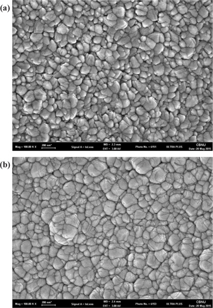
In Fig. 2, we have presented field emission-scanning electron micrographs (FE-SEM) of multi-layer solar absorber films with different gas mixture rate of Ar and (O2+N2).
Table 2 elucidates the deposition conditions of cermet multilayer coating, as shown in Fig. 2. From (a) to (c) in Fig. 2, the gas mixture rate of Ar and (O2+N2) was increasing in AlCrNO and AlTiNO cermet layer, respectively. All the surfaces were dark purple in color. As the gas mixture rate is increased, the grain size of cermet thin films grows up gradually in the resulting FE-SEM micrographs. In Fig. 2(c), it was observed that the surface showed large irregular particles that were pyramidal in shape. This is because the surface had not been nitridized due to low N2 flow rate. Moreover, an additional metallic phase also existed [7]. As shown in Fig. 2(a), (b), and (c), the grain sizes were approximately 42 nm, 66 nm, and 175 nm, respectively.
[Table 2.] Sputtering conditions of multi-layer cermet films as shown in Fig. 2.

Sputtering conditions of multi-layer cermet films as shown in Fig. 2.
Figure 3 shows FE-SEM images of multi-layer cermet films, containing an AlTiNO layer of varying dc power. The sputtering parameters of gas mixture rates are exactly same as the sample (c) conditions reported in Table 2. In the deposition process of AlCrNO layer, the dc power was 200 W. The grain size of multi-layer cermet films increased with an increase of dc power.
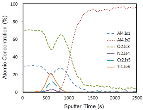
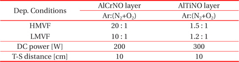
Figure 4 shows the AES depth profile analysis of Al2O3/AlTiNO/AlCrNO/Al multi-layer cermet absorber. Table 3 presents the deposition conditions of multi-layer coating, which is depicted in Fig. 4. In Al2O3 that serves as an antireflection layer, the gas mixture rate of Ar and O2 is fixed at 6 : 1.
[Table 3.] Sputtering conditions of multi-layer cermet films as shown in Fig. 4.
Sputtering conditions of multi-layer cermet films as shown in Fig. 4.
In the results of AES analysis, the depth profile displays the peaks of Al, O2, N2, Ti, and Cr elements. The profile coating consists of Al2O3 antireflection layer, AlTiNO and AlCrNO cermet multi-layer, and Al reflector layer extending from the surface to the substrate sequentially. The result of AES profile indicates that total thickness of multi-layer cermet films is approximately 240 nm. The concentration of Ti and Cr elements increases gradually, while the concentration of Al and oxygen elements decreases from the surface to the substrate. This trend essentially agrees well with the deposition conditions, as indicated in Table 3. From the surface to the substrate, the gas mixture rate of multi-layer increased sequentially. Consequently, the multi-layer was changed from LMVF to HMVF in AlTiNO and AlCrNO layer. Note that, oxygen is present as an element in all the layers. This can be ascribed to the high sensitivity of AES instrument. Furthermore, the oxygen contamination usually originates from the residual oxygen in a chamber.
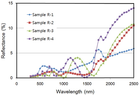
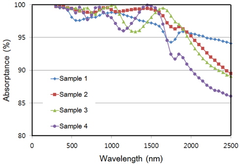
Figure 5 shows the absorptance spectra of a multi-layer cermet films, with various gas mixture rates of Ar and (O2+N2). Table 4 summarizes the sputtering conditions of AlTiNO and AlCrNO cermet films, which are illustrated in Fig. 5. Moreover, the absorptance of each sample was calculated using standard AM1.5 solar spectrum. All the absorptance curves of multi-layer cermet films approach values above 93%; however, slightly different traces are reported in the wavelength range of 0.3~2.5 μm. When the gas mixture rates were increased, the absorptance also showed a corresponding increase; the curve of this relationship has been elucidated and summarized in Fig. 5 and Table 4, respectively. On the other hand, Fig. 6 exhibits the reflectance spectra of multi-layer cermet films at different gas mixture rates. The reflectance curve exhibited a decreasing trend as the gas mixture rates were increased. The optimized value of optical properties is achieved in sample 1, having an absorptance of 95.5% and reflectance of 1.89%.
[Table 4.] Deposition conditions and optical properties of cermet samples as shown in Fig. 5.
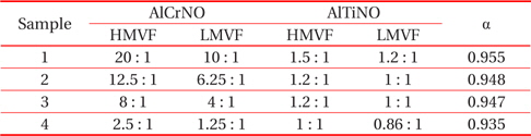
Deposition conditions and optical properties of cermet samples as shown in Fig. 5.
In this paper, we have described how to prepare a solar selective absorber. Five layers of the antireflection layer and multilayer, AlTiNO/AlCrNO cermet films, were subsequently deposited using a dc reactive magnetron sputtering system. The exact structure of As-deposited multi-layer films is Al2O3/AlTiNO (LMVF and HMVF)/AlCrNO (LMVF and HMVF)/Al/substrate. In the four absorbing cermet layers of AlTiNO/AlCrNO, the metal volume fraction was prepared using the controlling method of Ar and (N2+O2) gas mixture rate. As the gas mixture rate increases, the grain size of solar absorber films shows to grow up; the curve is illustrated in an SEM micrograph. Moreover, the grain size becomes larger as the dc power is increased. As the gas mixture rates were increasing, the absorptance also increased and the reflectance became low. The optimized value in sample 1 is achieved, with an absorptance of 95.5% and a reflectance of 1.89%.