There is a growing interest in the development of highaspect-ratio, three-dimensional (3D) structures in a variety of fields, such as 3D Fin FETs [1] and electromechanical resonator devices in the deep nanoscale range [2]. Over the years, various lithography techniques that are capable of patterning in the submicron scale and nanoscale have been developed. Electron beam lithography (EBL) [3], proton beam lithography [4, 5], extreme ultraviolet (EUV) lithography [6], and nano imprint lithography (NIL) [7] are a few among them. However, most of these lithographic techniques have been developed for the integrated circuit (IC) industry, which essentially deals with two-dimensional (2D) lithography.
One of the more common resists for EBL, poly (methyl methacrylate) (PMMA), can be used for the development of high-aspect-ratio 3D structures in the submicron/nanoscale. For example, a 3:1 aspect ratio (thickness=1 μm; minimum feature size=350 nm) submicron structure was formed in PMMA by EBL and was used as a resist mold for a metallic nanoscale electro thermal actuator [8]. However, the requirement of a large exposure dose, and thus, a long exposure time, to expose the thick PMMA film renders this material less attractive.
The development of an SU-8 epoxy-resin negative photoresist has facilitated the fabrication of high-aspectratio 3D structures by using conventional ultraviolet (UV) lithography in the micron scale. Good chemical and mechanical properties of cross-linked epoxy-based SU-8 have opened up a considerable number of new applications in the field of microelectromechanical systems (MEMS) [9]. With the use of this chemically amplified negative tone photoresist, devices with aspect ratios of approximately 20:1, features sizes in the range of tens of microns, and nearvertical sidewalls were developed [10].
Compared to a positive photoresist, such as PMMA, the negative tone photoresist SU-8 has many advantages; further, since it is a chemically amplified photoresist, it requires substantially low exposure doses. In addition, the added feature of direct write onto the photoresist for EBL or NIL eliminates the need for a mask. In this paper, we report the nanoscale patterning characterization of both EBL and NIL on SU-8.
II. ELECTRON BEAM LITHOGRAPHY ON SU-8
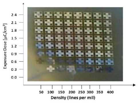
EBL was performed on a Texas Instruments EBL station setup custom-designed to work at an acceleration voltage of 20 kV. Three parameters (namely, density, exposure, and spot size) were available to the end-user for the characterization of any pattern/material. Spot size determines the width of the electron beam. Density defines the number of lines that are drawn to fill a unit length (1 mil=25.4 μm), while exposure defines the exposure rate in microseconds per unit length of the electron beam. A combination of the parameters exposure and density determine the total exposure dose (Q) that the photoresist is exposed to. The pattern is designed using computer-aided design (CAD) software and is then converted into the pattern description language (PDL) format that the EBL system reads. Additional lines that specify the values of exposure, density, and pattern repetition can be added to the PDL file. Spot size is varied by controlling the magnetic lenses that the electron beam passes through.
For the EBL experiment, a 3-inch silicon wafer was cleaned using a typical RCA cleaning procedure. A seed layer consisting of 100-Å chromium (Cr) and 1000-Å gold (Au) was sputter-deposited onto the wafer. Gold was chosen as the seed layer because of its excellent adhesion property to SU-8. In this study, commercially available Nano SU-8 2002 was selected to be used as the photoresist for the characterization. Spin-coating of SU-8 was carried out at 2,000 rpm for 30 seconds to obtain a photoresist thickness of approximately 1.65 μm. A two-step pre-exposure bake consisting of 60 seconds at 65℃ and 60 seconds at 95℃ on a hotplate was performed. After cooling to room temperature, the sample was exposed to the electron beam. A 2D array grid, shown in Fig. 1, with the exposure and density varying along each dimension was generated for each submicron pattern to be characterized. As shown in Fig. 1, the density values varied from 50 to 400 lines per unit length and the exposure values varied such that the exposure dose varied from 0.5 µC/cm2 to 2.5 µC/cm2 . Three different submicron spot sizes of 0.07, 0.13, and 0.25 micron were tried. Each of the spot sizes was used to expose the 2D grid successively.
After exposure, a two-step post-exposure bake consisting of baking on a hotplate at 65℃ for 1 minute and at 95℃ for 1 minute was carried out. The sample was then developed using the Nano SU-8 developer. The typical development time was about 60 seconds. Optimum development was verified by dipping the sample in isopropyl alcohol (IPA), which forms a white residue on the sample when underdeveloped. The developed sample was then rinsed in deionized water and dried. The developed sample was further cleaned by a short treatment of low-power oxygen plasma. During this process, about 0.15 μm of the surface SU-8 photoresist was etched back. This reactive ion etch (RIE) cleaning rendered a clean surface of the seed layer, thus promoting adhesion between the electrodeposited metallic layer and the metallic seed layer. After the RIE cleaning of the photoresist mold, the sample was dipped in an electroplating solution container and the container was placed in a low-vacuum chamber (approximately 500 mTorr) for about 30 minutes for removing any air bubbles trapped between the patterned nanoscale photoresist patterns. A plating current density of approximately 2 mA/cm2 was identified as the optimum rate for electroplating nickel for the fabrication of high-aspect-ratio submicron structures. The growth rate for this condition was about 2 μm/hr.
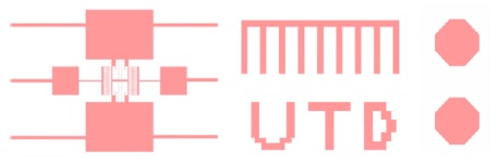
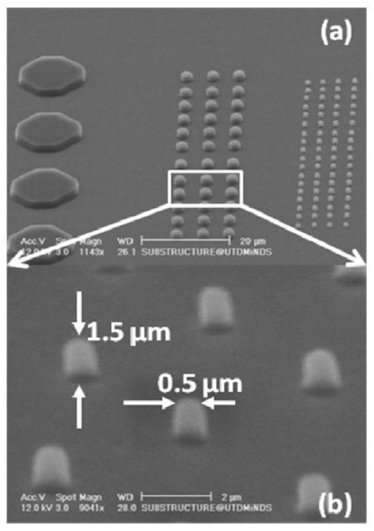
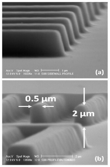
SU-8 2002 with two different process conditions was studied. The preliminary test patterns used for this characterization are shown in Fig. 2. Typical features sizes varied from 0.25 μm to 5 μm. These patterns were exposed onto 1.5- and 2-μm-thick SU-8 resists by using the exposure/density grids as described above. Among all the spot sizes used, the spot sizes of 0.07 μm and 0.13 μm rendered good patterns. The beam current for the 0.07-µm spot size was about 0.9 nA and about 2.9 nA for the 0.13-µm spot. As the exposure rate is a function of the beam current, the 0.13-µm spot beam was preferred over the 0.07-µm spot beam, thus achieving an exposure rate that is approximately three times faster.
Various test structures obtained from the optimized EBL for SU-8 are shown in Figs. 3 and 4. The required values of density and exposure are different not only for different patterns but also for different sections of the same pattern. Fine features need a low density value with a high exposure dose, while coarse structures, such as contact pads and anchors, need a high density value with a low exposure dose. These variations are incorporated into the PDL file. The cumbersomeness of this process can be avoided if the fine and the coarse features are separated and exposed sequentially with the same global parameters of exposure and density. The fine feature layer and the coarse feature layer can be aligned and exposed as two separate layers. This also enables the use of a relatively large spot size such as 0.75 µm with a current of 75 nA for the coarse features, thus further enhancing the write speed for the pattern.
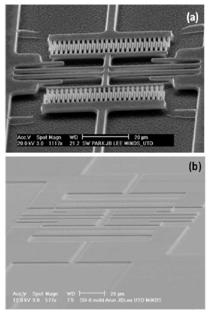
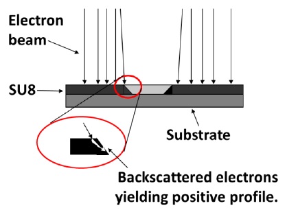
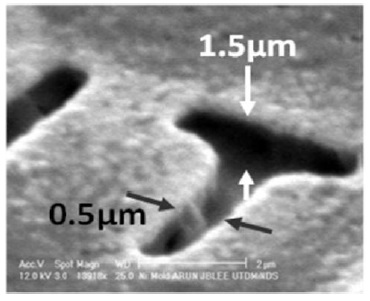
As a preliminary work to build structures, a comb-drive structure was fabricated using a well-established positive photoresist PMMA for the sake of comparison. A fully fabricated 1:1 aspect ratio submicron metallic comb-drive structure is shown in Fig. 5(a). A similar comb drive but with a relatively high-aspect-ratio (3:1) mold created in SU-8 is shown in Fig. 5(b). The exposure time for the PMMA mold was about 10 min, whereas that for SU-8 was about 30 seconds. The metallic structure in the case of PMMA was obtained by lift-off. The same process is not possible in SU-8 because of two distinct reasons. Firstly, the cross-linked SU-8 is difficult to remove in a solvent and the sidewall profile has an inherently positive slope in the case of a negative photoresist and an inherently negative slope for a positive photoresist for EBL. Solubility in a solvent and the negative sidewall profile of the photoresist are essential for obtaining good lift-off structures. This inherently positive sidewall profile for negative resists and negative sidewall profile for positive resists can be attributed to the backscattering of incident electrons. Fig. 6 shows a schematic representation of the behavior of the backscattered electrons in a negative photoresist.
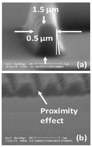
A closer look at the sidewall pattern of SU-8 shown in Fig. 7(a) clearly indicates the slightly positive profile due to the backscattered electrons from the substrate. This effect is not problematic when the separation between patterns is not in the deep submicron range. When the patterns are placed very close to each other, the backscattered electrons tend to combine and the distortion in the pattern is more pronounced. This effect is known as the proximity effect in EBL. The distortion of structure due to this effect is shown in Fig. 7(b).
The electroplating of nickel was done initially in the form of growing mold structures around SU-8 structures. Fig. 8 shows nickel molds electroplated onto SU-8 structures. Submicron SU-8 molds experience a considerably severe proximity effect when compared to the submicron SU-8 structure as the exposure area for the mold structure is relatively large. This makes the plating of nickel molds easier than the growth of nickel structures.
III. NANOIMPRINT LITHOGRAPHY ON SU-8
Although the processing time for the formation of nanoscale structures by using EBL is not prohibitively long in practice, it is desirable to have in place a fabrication process that can pattern nanoscale structures within a relatively short process time. To reduce the process time significantly, we studied an alternate method of the formation of nanoscale patterns using NIL. In this study, we used two different nano grating silicon molds, one with 10-nm-wide grating and 100-nm pitch distance and the other with 20-nm-wide grating and 200-nm pitch distance. Note that the minimum feature size studied for the NIL is approximately 50 times smaller (from 500 nm in EBL to 10 nm in NIL), but the NIL allows a limited density range as it requires a good gap between the features (100-nm pitch distance in our case).
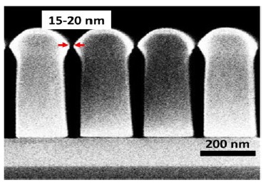
The fabrication was started by spin-coating a layer of 450-nm-thick SU-8 on an oxidized silicon wafer with 2-μm oxide, and the SU-8 layer was imprinted with a 20-nm-wide, 200-nm-pitch nano grating mold. 200-Ǻ-thick Cr was evaporated on the imprinted SU-8 gratings at an oblique angle of 35°. Plasma etching in oxygen was carried out at 5 mTorr with an inductively coupled plasma (ICP) power of 300 W and a bias power of 100 W for 60 seconds to etch the exposed SU-8. The Cr layer was etched using a Cr etchant (a solution of 20 g:20 g:100 mL of NaOH:K3Fe(CN)6 :H2O). Fig. 9 shows a scanning electron microscopy (SEM) image of the cross-section of the imprinted and etched SU-8 structure, showing 30:1 aspect ratio 15- to 20-nm-wide openings at the top. During plasma etching, there was a slight widening of the nanoscale patterns beyond the dimension of the top opening in the imprinted SU-8. However, due to the highly directional nature of ICP etching, the transferred dimension at the bottom of the trench was not significantly different from the topmost dimension.
Although 30:1 aspect ratio nanoscale patterning with a minimum feature size of 15–20 nm was successful, we investigated further to find a recipe for achieving sub-10-nm patterns. In order to make sub-10-nm-wide opening patterns, a method involving the evaporation of a metal at oblique angles of more than 35° or the use of a relatively thick metal mask could be used. In our study, another alternative method was investigated. An additive 45-nm-thick SiO2 layer was evaporated on the imprinted and etched SU-8 membrane at an oblique angle of 35°. Fig. 10 shows an SEM image of the cross section of the imprinted and etched SU-8 membrane with 45-nm-thick SiO2 at the top, showing the smallest dimension down to 7-nm-wide openings. However, the dimension varies from one region to another and a reproduction of the nano slots with uniform openings at the top of the etched SU-8 membrane was practically impossible because the metal or dielectric material evaporation rate in the electron-beam evaporator was not uniform. Nonetheless, this study demonstrated nanoscale patterns with aspect ratios of up to 64:1 (thickness=450 nm; minimum feature size=7 nm).
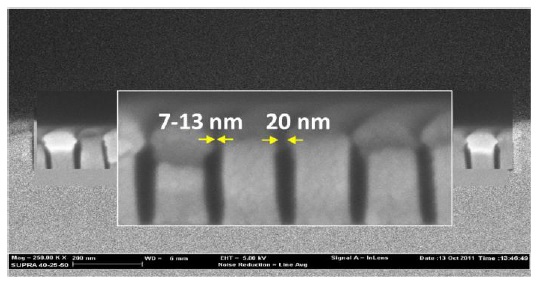
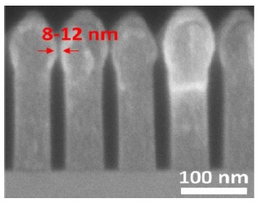
Since the additive layer of the oblique-angle deposited SiO2 was not uniform, a further study was carried out to find a method of realizing uniform sub-10-nm patterns in SU-8. To make uniform sub-10-nm-wide openings, the 10-nmwide, 100-nm-pitch nano grating silicon mold was fabricated and tested. First, SU-8 2000.5 and SU-8 2000 thinners were mixed in a 4:1 ratio. A layer of 300-nm-thick diluted SU-8 was spun on an oxidized silicon wafer with 2-μm buried oxide and imprinted with the 10-nm-wide, 100-nm-pitch nano grating mold. Cr was evaporated on the imprinted SU-8 gratings at an oblique angle of 35°. Then, oxygen plasma etching was carried out at 5 mTorr with an ICP power of 300 W and a bias power of 100 W for 55 seconds, and a Cr layer was etched using a Cr etchant. Fig. 11 shows an SEM image of the cross section of the imprinted and etched SU-8 membrane showing 8- to 12-nmwide openings at the top resulting in aspect ratios of up to 37.5:1. Like the 20/200-nm mold NIL, this 10/100-nm mold NIL was reproducible and consistently led to the sub-10-nm patterning result with a minimum variation of sizes.
Deep submicron to sub-10-nm feature patterning was studied on a negative tone chemically amplified photoresist using both EBL and NIL. Submicron structures with an aspect ratio of 4:1, a minimum feature size of 500 nm, and near-vertical walls were obtained using EBL. Various process condition variations for different types of patterns were discussed. In the NIL, reproducible nanoscale patterning down to 8 nm with an aspect ratio of up to 37.5:1 was demonstrated. These two methodologies show considerable potential of the nanoscale patterning ability in a negative photoresist. We believe that such methods can be widely applicable to the development of 3D FinFETs and nanoscale multifunctional devices.