Carbon-nanotube field-effect transistors (CNFETs) have attracted considerable attention as a potential alternative to the silicon complementary metal-oxide semiconductor (CMOS) process. Similar to CMOS, CNFETs are fieldeffect transistors but use one or many carbon nanotubes (CNTs) as the transistor channel instead of bulk silicon. Among the many potential alternatives to the CMOS process, CNFET has attracted attention because of its significant power–performance benefits [1]. In terms of performance, [2] reports that CNFET circuits are about two to ten times faster and that energy consumption is about two to seven times lower. Thus, CNFETs can achieve a 20× energy-delay product. In [3], the authors demonstrated a 9-nm CNFET fabrication showing that scaling can be done in both CNFET circuits and CMOS circuits. Many studies have provided solutions to the yield and reliability problems related to CNFETs. [4] proposed a promising way to remove metallic CNTs for improved reliability, and [5] described ways to improve the CNFET yield. In addition, CNFET circuits were fabricated [6] to show that CNFETs may replace CMOS in the near future.
Thus far, however, no study has answered the following question: “If CNFET is such a good candidate to replace CMOS, what would be the benefit of CNFET very largescale integration (VLSI) over CMOS at the full-chip scale?” In this study, we attempt to answer this question. Therefore, in this paper, we propose a methodology for designing a full-chip CNFET circuit by using the latest CNFET technology models and compare the performance benefits with those of CMOS in an actual layout. We propose a methodology and an algorithm for extracting parasitic elements from a CNFET circuit in order to accurately analyze its performance; further, we compare the full-chip performance of CNFET with that of CMOS and show the impact of applying a future CNFET technology (CNT density: 200 CNTs/µm) to CNFET circuits.
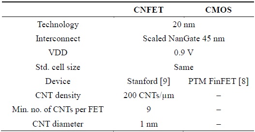
In this paper, we provide the design methodology and the analysis results for two technology designs: 45 nm and 20 nm. The details of and assumptions about the technology that we use for the 45-nm design analysis are presented in Table 1 (the 20-nm design analysis is described in Section V). First, we choose predictive technology model (PTM) 45-nm high-k/metal gate for low-power applications (PTM LP 45 nm) as our baseline CMOS technology [7] (a 20-nm CNFET is compared with a 20-nm FinFET [8]). Second, we assume that CNFETs have the same interconnect structure as CMOS. Despite the fact that the interconnect in a CNFET can be optimized differently from that of a CMOS for its best performance, we choose the same in this study for a fair comparison between CNFET and CMOS. Third, we assume the same VDD of 1.1 V. Fourth, we use Stanford’s model for our CNFET simulations [9]. Fifth, we assume a CNT density of 200 CNTs/µm. A density of 200 CNTs/µm is reported as the future goal for achieving the best performance of CNFET fabrication [10]. Sixth, the standard cell sizes for CMOS and CNFETs are designed to be the same. We do not consider the possibility of different standard cell sizes of CNFETs and CMOS in our study. Finally, we assume that a minimum of 10 CNTs is needed per CNFET for reliability.
[Table 1.] 45-nm technology settings used in this study
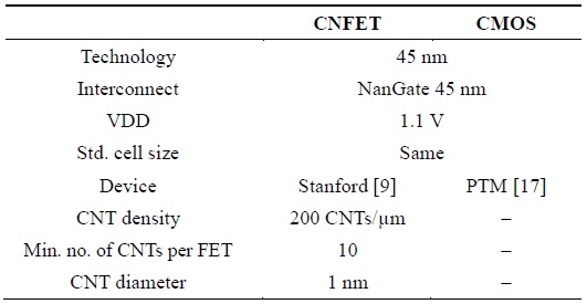
45-nm technology settings used in this study
We believe that our assumptions are reasonable on the basis of the following references:
Many researchers have reported that the contact resistance between CNTs and the metal in CNFETs can be significant [12]. However, in this study, we assume that the problem of significant contact resistance is solved because of the following reason: in [13], with the use of a carbon nanotube-graphite interface, the contact resistance was reduced significantly. Further, [14] actually demonstrated this technique and showed a significant reduction in the contact resistance.
In this study, we also assume that metallic CNTs do not impact our CNFETs, and most of the yield problems are resolved. Many researchers [15, 16] have reported that metallic CNTs can be successfully removed (99.99%) during fabrication. Since our focus is on studying the design and performance advantage of CNFETs over CMOS, and knowing that many researchers have already provided solutions to the CNFET yield problems, we will not focus on reliability issues that have already been resolved as we follow the guidelines from an actual functioning CNFET design [6].
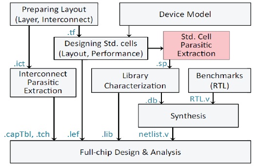
A major advantage of our full-chip CNFET design methodology is that as far as possible, we implement our flow by using the existing electronic design automation (EDA) tools. Fig. 1 shows the relevant details. First, we choose the interconnect structure and generate a .tf file and an .ict file. We use the .tf file to design the standard cells in Cadence Virtuoso and the .ict file to extract the parasitic elements of the interconnect by using Cadence QRC Techgen (.capTbl and .tch). Second, we design the standard cells on the basis of the design rules and the new device (CNFET) performance. Upon the completion of the standard cell design, we extract the parasitic elements of these cells (the relevant details are provided in Section III). Then, we insert the standard cell netlist with the parasitic elements into Synopsys SiliconSmart for characterization (.db and .lib). Finally, we synthesize the benchmarks (RTL.v) by using Synopsys Design Compiler (netlist.v) and then perform the full-chip design and analysis by using Cadence SoC Encounter. Note that no currently existing tools can extract the parasitic elements in CNFETs. In the following section, we discuss in detail our approach to this problem.
III. CNFET PARASITIC EXTRACTION
Parasitic extraction is a very important part of full-chip design and analysis. We categorize this into three parts: interconnect-to-interconnect, device-to-interconnect, and internal device. Interconnect-to-interconnect parasitic elements are resistances and capacitances between interconnects. Device-to-interconnect is the coupling capacitance between devices near the interconnects and other parasitic elements such as interconnect-to-CNTs. Internal-device parasitic elements are the ones that affect the device performance.
Internal-device parasitic elements have been analyzed and implemented well in the device model that we use in this study [2, 17]. Therefore, we do not consider them in our work. For interconnect-to-interconnect parasitic elements, despite the fact that CNFET is a new device, the existing EDA tools (such as Synopsys StarRC and Cadence QRC Extractor) can extract the parasitic elements accurately unless novel interconnect materials are added (such as CNT interconnects). However, the existing EDA tools cannot handle device-to-interconnect parasitic elements in CNFETs because of the CNTs inside the devices. Therefore, we focus on extracting the device-to-interconnect parasitic elements.
Device-to-interconnect parasitic extraction in CNFET is a challenging task because of two reasons. First, the existing EDA tools cannot handle this directly. Three-dimensional electromagnetic (3D EM) solvers can handle CNT parasitic extraction but not at the full-chip scale, and full-chip EDA tools cannot handle the CNTs inside their engine. Second, the parasitic capacitance of a CNFET varies within a wide range on the basis of the geometry and density of the CNTs.
We use the following steps to tackle this problem. First, we expect that the parasitic capacitance values are different for different CNT densities. Thus, we first fix the CNT density parameter (e.g., 50 CNTs/µm) and observe the similarities and differences between CMOS and CNFET. Knowing that the only difference between CMOS and CNFET is how the channel is formed, we propose the application of a scaling factor to CNFETs by using the existing computer-aided design (CAD) tools.
Therefore, on the basis of these properties, we propose a methodology for extracting parasitic elements by using Mentor Graphics Calibre PEX and Synopsys Raphael. To do this, we use a two-step approach. First, Calibre PEX extracts the parasitic elements of a CNFET layout in which the CNT layers are replaced by metal planes. For example, for an inverter that consists of two CNFETs, in the two parts where CNTs form the channel of a CNFET, the CNTs are replaced with a simple metal plane during extraction. Then, we apply the scaling factors obtained from Synopsys Raphael to the extracted parasitic elements. Notice that the metal plane and the CNTs have different structures. However, with numerous layout simulations, we show that a scaling factor exists between them, and thus, we can successfully extract the device-to-interconnect parasitic elements from the CNFETs. We focus our efforts on capacitance extraction because all other parasitic elements (such as R or L) are either modeled inside the device or will not change in a CNFET; hence, the existing tools can handle them.
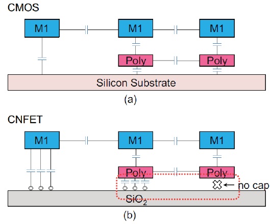
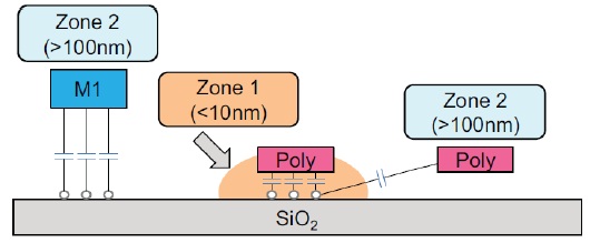
Algorithm 1 describes the details. First, given the CNT density (e.g., 50 CNTs/µm), we extract the parasitic capacitance of the layout assuming that the CNT layer is a metal plane. For example, a CNT layer that has 10 CNTs within a length of 100 nm is converted into a metal plane measuring 200 nm (pitch: 20 nm × 10) × 100 nm. Then, for an extracted capacitance between the metal planes, we sort this into N zones on the basis of its capacitance value. If the extracted capacitance is in the range of the capacitance expected in a certain zone, we apply the scaling factor of this zone. If not, we retain its value. In short, for the capacitance between CNTs and the metal, we apply scaling factors on the basis of its capacitance value extracted using Calibre PEX. We find that only the CNT-to-metal (poly and M1) capacitance is impacted significantly by the CNTs in the CNFETs. Note that the change in the coupling capacitance between interconnects (e.g., M1-to-M1 and poly-topoly) is almost negligible. By comparing Fig. 2(a) and (b), we find that the only difference between CMOS and CNFET is the capacitance between the metal (poly) and the substrate (SiO2). In CNFETs, unlike in CMOS, a negligible capacitance is generated between the metal and the substrate.
[Algorithm 1.] CNFET parasitic capacitance extraction
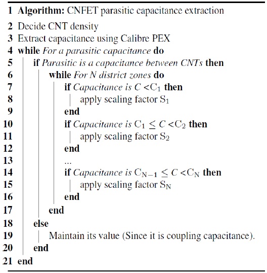
CNFET parasitic capacitance extraction
We verify that our method is very accurate and has a reasonable error. In Fig. 3, we illustrate the separation of the scaling factor zones in our interconnect structure. For poly, the minimum distance between poly and CNTs is less than 10 nm when poly is right on top of the CNTs. However, a poly that does not face the CNTs directly below it will have a minimum distance of 100 nm between the CNTs because of the design rules. In the case of M1, the closest distance that M1 can have to a CNT is more than 100 nm. Therefore, because of the design rules and the interconnect geometry, we separate our scaling factors into two zones (N = 2). We now know that a metal (poly or M1) will be either as close as <10 nm to the CNTs (Zone 1) or farther than 100 nm (Zone 2). Therefore, we generate two scaling factors. We do not generate additional zones that are more than 100 nm away because the scaling factor converges to 1 (Table 2). If the design rules of a technology allow a metal to be designed inside a zone that is 10 nm< x < 100 nm, we must have more zones for an accurate analysis.

Scaling factors used for device-to-interconnect parasitic elements in CNFET circuits (45 nm)
Our scaling factors are based on the results of the 3D EM simulation (Synopsys Raphael, ver. D-2010.03). In each zone, we generate random structures that are identical for the metal planes and the dense CNTs (e.g., CNTs with a density of 50 CNTs/µm). For example, a random structure for dense CNTs consists of one poly and a random number of CNTs (e.g., 10 CNTs), and the corresponding structure for the metal plane consists of a poly and a metal plane that has an equivalent area of the abovementioned CNT structure (10 CNTs × 20-nm pitch). Since Zone 2 has more possible structures for parasitic extraction, we generate 100 random structures for Zone 1 and 200 for Zone 2 on the basis of the design rules of the layout. In our experiments, CNTs are assumed to be dealt as a metal in a material since Synopsys Raphael cannot handle CNTs in its extraction.
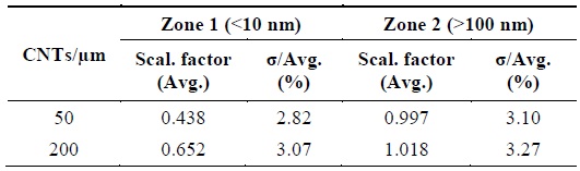
Table 2 shows our results. We choose scaling factors on the basis of the average values from our experiments. In the case of a CNT density of 50 CNTs/µm, the capacitance of CNTs to the metal in Zone 1 is only 44% of the metal plane. However, in Zone 2, the scaling factor is 0.997, implying that the capacitance impact of the CNTs in this zone is not very significant. On the basis of this trend, the scaling factor converges to 1 as the distance increases. When the CNT density is 200 CNTs/µm, the scaling factor in Zone 1 is larger than that in the case of a density of 50 CNTs/µm (0.652 < 0.438), but considering that 4× more CNTs are inside the same area, this is not a significant increase. Scaling factors in Zone 2 for the densities of 200 CNTs/µm and 50 CNTs/µm show that the impact of the CNFET parasitic elements will not be significant if the CNFETs are far away from the interconnect. The σ/Avg. values of our simulations show that the proposed method is very accurate and has a small variation. In all simulations, the σ/Avg. values for the proposed method were smaller than 3.3%.
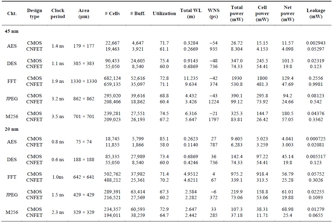
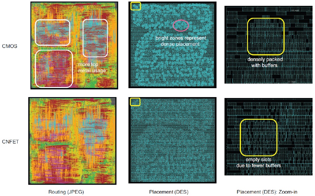
We summarize our layout results in Table 3 (the detailed results are presented in Table 8); Fig. 4 shows the layout shots of the difference between CNFET and CMOS. All designs meet the timing requirements, and the results are based on the fastest clock period that the CMOS circuits can meet. First, the CNFET circuits outperform the CMOS circuits in terms of both timing and power. Note that the CNFET designs show a significant positive timing slack. For example, DES has the worst negative slack (WNS) of +736 ps. This implies that the critical path delay of the DES design is not 1.1 ns but 0.364 ns, and it could be further optimized for better timing. In terms of power, we see 4.67× improvement in CNFET over CMOS. Second, we see a significant reduction in the standard cell count (–19.7%) and the buffer count (–34.4%) on average. Since CNFETs have faster devices, they require fewer cells and smaller wire length to achieve the same benchmark (see Fig. 4). The relatively low cell count, buffer count, and wire length translates to additional power reduction in CNFET circuits.
[Table 3.] Full-chip results for 45-nm 200-CNTs/μm designs
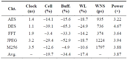
Full-chip results for 45-nm 200-CNTs/μm designs
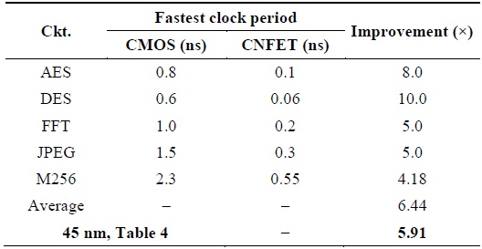
To visualize the timing benefits of CNFETs, we design benchmarks that run on the fastest-possible clock period and estimate how significant the timing benefit that we can achieve with CNFET circuits is. From Table 4, we infer that 200-CNTs/µm designs can achieve an average of 5.91× improvement in the clock period. Because CNFET cells are significantly faster than CMOS cells, we obtain a significant performance gain over CMOS in 200-CNTs/µm designs.
[Table 4.] Clock period reduction between CMOS and CNFET (45 nm)
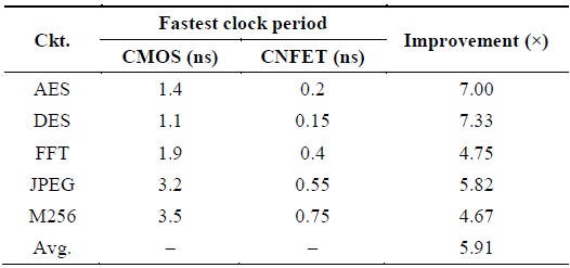
Clock period reduction between CMOS and CNFET (45 nm)
We will describe our 20-nm technology setup before reporting our results. In this 20-nm analysis, we also try our best to design CMOS and CNFET libraries that are similar to each other for a fair comparison. Details of the 20-nm technology setup are given in Table 5. First, we use the PTM-MG 20-nm LSTP [8] model for CMOS (FinFET), and Stanford’s model for CNFET [9]. The VDD for both is 0.9 V. Since Stanford’s CNFET model is scalable and has many parameters to adjust, we scale only the parameters related to the physical dimensions. In other words, parameters that can improve CNFET performance without any change in the size were not modified (e.g., Vth). In the case of the 20-nm technology, we will assume our reliability limit (5-nm pitch × 9 = 45 nm) to be nine CNTs for the same standard cell sizes for 20-nm CMOS and CNFET. Second, we scale the interconnect dimensions down to (20/45)× = 0.44×. On the basis of this scaling factor, we rebuild the interconnects and the interconnect libraries. With respect to resistance, since many researchers have reported the resistivity increase due to the relatively small interconnects, we recalculate the resistance of our interconnects by using the equations given in [18]. Third, we scale down the shapes of our standard cells by 0.44×. We still ensure that the sizes of the CMOS and CNFET standard cells are the same. Thus, we develop our 20-nm CMOS and CNFET libraries.
[Table 5.] 20-nm technology settings used in this study
20-nm technology settings used in this study
We summarize the results for the 20-nm design in Table 6 (detailed results are presented in Table 8). Benchmarks are synthesized in the 20-nm design, and both CMOS and CNFET start from the same synthesized benchmark. First, we see similar trends of timing and power reduction in both 20-nm and 45-nm designs. The cell count reduces by 24%, and the buffer count reduces by 52%. The wire length reduces by 10%, and we observe significant timing slacks in the CNFET benchmarks. Note that the reduction ratio in the cell, buffer, and wire length is different from those in the 45-nm design, but this is because benchmarks that are synthesized different are based on designs that show different improvements. However, we do observe a clear trend that CNFET outperforms CMOS. Second, we see a 3× power improvement as compared to CMOS in the case of the 20-nm design. However, the power benefit in the case of the 45-nm design was 3.9×. Next, we will discuss why CNFET seems to be losing its power benefit in the case of the 20-nm design. In the case of the 45-nm design, the CMOS model that we used was the PTM LP model with a planar gate. However, for the 20-nm design, PTM-MG acts as the FinFET. Significant advances in device performance were made in the 20-nm CMOS, and the <20 nm models used for comparison in the previous studies were based on planar CMOS devices [12].
[Table 6.] Full-chip results for 20-nm 200-CNTs/μm designs. Values represent a reduction from CMOS
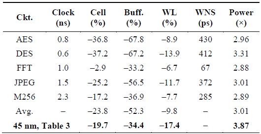
Full-chip results for 20-nm 200-CNTs/μm designs. Values represent a reduction from CMOS
Despite the reduced power benefit as compared to the 45-nm design, CNFET still has a significant power benefit over CMOS. In summary, we report that CNFET outperforms CMOS in terms of various metrics in both the 20-nm and the 45-nm designs.
We perform the same simulations as shown in Table 4 to see the timing benefit in the 20-nm CNFET. We design the CNFET benchmarks to run at the fastest clock period. In Table 7, we report that the 20-nm CNFET shows a 6.4× improvement in the clock period. This is a similar to the trend observed in the case of the 45-nm design, and we conclude that the CNFET shows a significant delay benefit over CMOS for both the 45-nm and the 20-nm designs. Overall, through this study, we report that the CNFET shows a maximum delay/power benefit of 22.8× in the case of the 45-nm design, and 19.4× (6.44 × 3.01) in the case of the 20-nm design.
[Table 7.] Clock period reduction between CMOS and CNFET (20 nm)
Clock period reduction between CMOS and CNFET (20 nm)

20-nm technology
Based on our findings for the 45-nm and 20-nm full-chip designs, we predict the following future technology impacts of CNFETs over CMOS:
In this paper, we proposed a methodology for designing full-chip CNFET circuits and demonstrated the power/delay benefits of CNFETs over CMOS in 45-nm and 20-nm technology. We proposed a methodology and an algorithm for accurate parasitic extraction and found out that because of its device structure, CNFET could gain a significant improvement in terms of power and delay. In terms of the full-chip results, in the 45-nm design, CNFET circuits achieved 5.91 × /3.87 × (delay/power) benefit at a CNT density of 200 CNTs/µm. In the case of the 20-nm design, CNFET achieved a 6.44 × /3.01 × (delay/power) benefit over CMOS at a CNT density of 200 CNTs/µm. On the basis of our study, we predict various advantages that nanometerscale CNFETs will have over CMOS. In particular, we expect to see a significant power/performance benefit of CNFET over CMOS in more advanced technology nodes as well.