Zinc oxide varistor ceramics are attractive and smart materials, which reveal the nonlinearity in the voltage-current relation [1]. The nonlinearity is attributed to a distinctive microstructure with many grains and active grain boundaries [2,3]. A unit microstructure composed of grain-grain boundary-grain is distributed to the entire bulk with a 3-dimensional series and parallel connection [2,3]. Pure zinc oxide also has many grains and grain boundaries, and each grain boundary is not active. Thus, zinc oxide exhibits a linear voltage-current relation dominated by ohm’s law.
Zinc oxide varistor ceramics incorporated with various additives exhibit V-I characteristics similar to a back-to-back Zener diode, with non-conduction state below breakdown voltage and conduction state above breakdown voltage [3]. They are extensively utilized to protect circuit devices from incoming surge from the external environment.
Commercial zinc oxide varistor ceramics incorporated with bismuth and praseodymium should be sintered at a high temperature above 1,000℃ [1,4]. Therefore, the chip type varistor ceramics must use a refractory of high melting point such as palladium and platinum as an inner-electrode. Palladium and platinum are expensive when compared with various other metals. Zinc oxide ceramics incorporated with vanadium can be sintered even at temperatures as low as 900℃, and exhibit a nonlinear property [5,6]. The advantage of this is that silver can be used as an inner-electrode, instead of palladium and platinum. Nevertheless, it is difficult to use these varisors commercially because of their large number of unsolved problems [7-15]. Therefore, it is interesting to explore how the sintering process has an effect on the varistor properties for a specific composition. In this work, the sintering effects on microstructure, electrical properties, and dielectric characteristics of ZnO-V2O5-MnO2-Nb2O5-Dy2O3-based ceramics were investigated at a temperature as low as 875~950℃.
High-purity (>99.9%) reagent-grade raw materials were prepared and utilized in the proportions of 97.35 mol% ZnO (Aldrich chemical com., USA) + 0.5 mol% V2O5 (Kojundo chemical Lab., Japan) + 2.0 mol% MnO2 (Kojundo chemical Lab., Japan) + 0.1 mol% Nb2O5 (Kojundo chemical Lab., Japan) + 0.05 mol% Dy2O3 (Kojundo chemical Lab., Japan). Raw materials were blended with zirconia balls and acetone in a polypropylene bottle for 24 h using a ball mill. The blend was dried at 120℃ for 12 h, and the dried mixture was then blended with acetone and polyvinyl butyral binder (0.8 wt% based on powder weight) in a beaker using a magnetic stirring bar. After drying at 120℃ for 24 h, the starting powder was produced by granulating the blend by sieving through a 100-mesh screen. A pressure of 100 MPa was applied to press the powder into disk-shaped pellets of 10 mm in diameter and 1.3 mm in thickness. The pellets were set on a MgO plate in an alumina sagger, sintered at different temperatures (875, 900, 925, and 950℃) in air for 3 h, and then left to cool to room temperature. The heating and cooling rates were at 4℃/min, and the final pellets were of ~8 mm in diameter and 1.0 mm in thickness. A conductive silver paste was coated on both faces of the pellets by using screen-printing techniques, and electrodes of 5 mm in diameter were formed by heating at 550℃ for 10 min. Finally, the lead wire was soldered to both electrodes, and the samples were packaged by dipping them into a thermoplastic resin powder.
2.2 Microstructure examination
One side of the samples was lapped and ground with SiC paper, and was then polished with 0.3 μm-Al2O3 powder. The polished samples were chemically etched in a HClO4-H2O solution (1:1,000, v/v) for 25 s at 25℃. The surface microstructure was examined using a field emission scanning electron microscope (FESEM, Quanta 200, FEI, Brno, Czech). The average grain size (d) was determined using the lineal intercept method with the expression d = 1.56 L/MN, where L is the random line length on the micrograph, M is the magnification of the micrograph, and N is the number of grain boundaries intercepted by the lines [16]. The crystalline phases were identified using an X-ray diffractometer (XRD, X'pert-PRO MPD, Panalytical, Almelo, the Netherlands) with CuKα radiation. The density (ρ) of the sintered pellet was measured using a density determination kit (238490) attached to a balance (AG 245, Mettler Toledo International Inc., Greifensee, Switzerland).
The electric field (E)-current density (J) characteristics were measured using a high voltage source-measure unit (Keithley 237, Keithley Instruments Inc., Cleveland, OH, USA). The breakdown field (EB) was measured at a current density of 1.0 mA/cm2 and the leakage current density (JL) was measured at 0.80 EB. The non-ohmic coefficient (α) was defined using the empirical law, J = C·Eα , where J is the current density, E is the applied electric field, and C is a constant. α was determined through the expression, α = 1/(logE2-logE1), where E1 and E2 are the electric fields corresponding to 1.0 and J2 = 10 mA/cm2 , respectively.
2.4 Dielectric characteristic measurement
The dielectric behavior, in accordance with frequency for the apparent dielectric constant (εAPP') and dissipation factor (tanδ) of the samples, was measured in the range of 100 Hz-2 MHz using an RLC meter (QuadTech 7600, Marlborough, MA, USA).
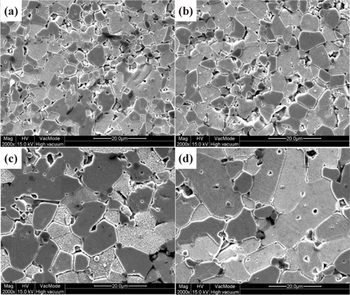
Figure 1 shows SEM micrographs of the samples sintered at different temperatures. Clearly noticeable grain boundaries and diverse grain sizes are distributed throughout the entire bulk. On the whole, no remarkable difference was observed when compared with the surface morphologies of other ZnO-V2O5-based varistor ceramics [13-15]. However, it can be seen that the grain size noticeably increased despite a change of as small as 75℃ in the total range of the sintering temperature. In particular, the grain size increased abruptly when the sintering temperature exceeded 925℃.
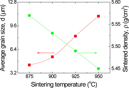
The tendency of change in the average grain size (d) and the density (ρ) of the sintered pellets as a function of sintering temperature is indicated graphically in Fig. 2. With the increase of sintering temperature, d increased remarkably from 4.3 to 10.9 μm and ρ decreased from 5.57 to 5.45 g/cm3 (pure ZnO, theoretical density = 5.78 g/cm3). It is worth noting that the ceramics with this composition can be sintered at a temperature as low as 875℃. This is assumed to be because of the volatility of the V-species for V2O5 with low melting point as low as 690℃.
Figure 3 shows the XRD patterns of the samples sintered at different temperatures. Minor phases such as Zn3(VO4)2, ZnV2O4, DyVO4, and VO2 were detected as secondary phases. The secondary phases were produced by the following chemical reaction.
3ZnO + V2O5 → Zn3(VO4)2
ZnO + V2O5 → ZnV2O4 + O2
Dy2O3 + V2O5 → 2DyVO4
V2O5 → 2VO2 + (1/2)O2
Among minor phases, VO2 (2 θ = 28.0650) almost disappeared when the sintering temperature exceeded 900℃. Also, the peak of ZnV2O4 reduced gradually with the increase of sintering temperature. However, the peaks of Zn3(VO4)2 and DyVO4 did not vary with the increase of sintering temperature. The reduction of the ZnV2O4 and VO2 peaks may therefore affect the nonlinear properties. The microstructure characteristic parameters are summarized in Table 1.
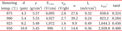
Average grain size (d), sintered density (ρ), breakdown field (EB), breakdown voltage per grain boundary (vgb), nonlinear coefficient (α), leakage current density (JL), dielectric constant (εAPP'), and dissipation factor (tanδ) of the varistor samples for different erbium amounts.
Figure 4 shows the electric field-current density (E-J) characteristics of the samples sintered at different temperatures. The varistor is a type of voltage switcher that senses a critical voltage. Therefore, the characteristic curves are divided into two states based on critical voltage: off-state due to extremely high resistance before critical voltage and on-state due to extremely low resistance after critical voltage. However, the shape of the edge between the off-state and on-state somewhat differs with sintering temperature.
The breakdown field (EB) showed an abrupt tendency of change from 6095 to 996 V/cm with the increase of sintering temperature. EB is mainly controlled by the average grain size (d) and it weakly depends on the breakdown voltage per grain boundary (vgb). The breakdown voltage (VB) is indicated through the expression, VB = (D/d)·vgb = n·vgb. As a result, EB is written as follows: EB = vgb/d, where d is the average grain size, D is the thickness of sample, and n is the number of grain boundaries [2]. As a result, the decrease of EB with the increase of sintering temperature is attributed to the increase of the average ZnO grain size and the decrease of breakdown voltage per grain boundary.
The tendency of change in the nonlinear coefficient (α) as a function of sintering temperature is shown graphically in Fig. 5. α increased from 27.6 to 40 until the sintering temperature reached 900℃. When the sintering temperature exceeded 900℃, α decreased to below 10, and a further increase in sintering temperature again increased α. α exhibited fluctuation in the tendency of change with the increase of sintering temperature. In light of the tendency of change in α, the sintering temperature has a noticeable effect on nonlinear properties despite small sintering changes. It is worth noting that the sample sintered at a temperature as low as 875℃ exhibited a α value reaching α =27.1. This suggests a potential possibility at low temperature sintering. The behavior of α in accordance with sintering temperature is related to the potential barrier height, which strongly depends on the electronic trap states, such as the zinc vacancies (VZn), interstitial zinc (Zni), ionized donor-like (DZn) oxygen (Oi ), etc. at the grain boundaries [22]. Furthermore, these defects will be affected by sintering temperature. As mentioned in the XRD analysis, minor phases such as ZnV2O4 and VO2, in particular VO2, were affected by the sintering temperature exceeding 925℃. It is strongly assumed that this may change the density of interface states, in light of the decrease of the nonlinear coefficient.
The tendency of change in the leakage current density (JL) as a function of sintering temperature is indicated graphically in Fig. 5. It can be seen that JL exhibited a fluctuation with the increase of sintering temperature. When the sintering temperature increased, JL decreased from 0.32 to 0.24 mA/cm2 until the sintering temperature reached 900℃, and then increased in the range of 0.36~0.49 mA/cm2 when the sintering temperature was further increased. On the whole, α and JL exhibited each other’s opposite tendency of change, as can be seen in Fig. 5. The E-J characteristic parameters are summarized in Table 1.
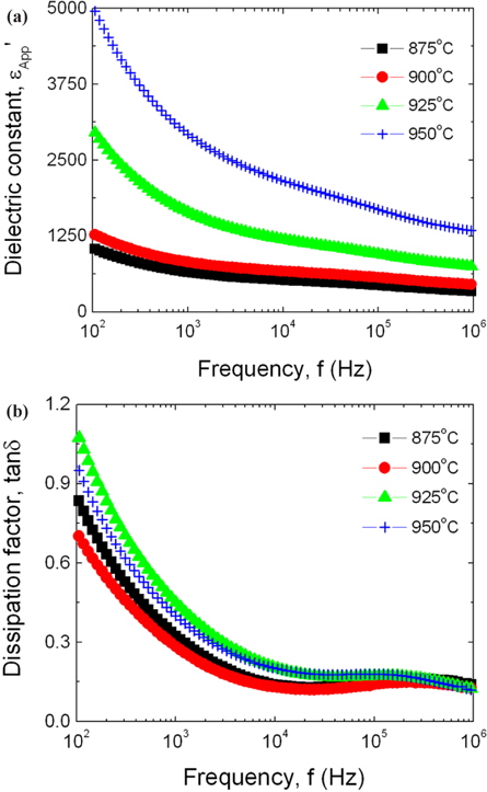
Figure 6 shows the apparent dielectric constant (εAPP') and dissipation factor (tanδ) of the samples sintered at different temperatures. εAPP' for all the samples shows a typically dielectric dispersion phenomenon, which decreases with increasing frequency. The decrease of εAPP' with increasing frequency is assumed to be a result of the decrease of the number of electric dipole, which can follow to gradually increasing frequency. The variation rate of the dielectric dispersion was remarkably large at below 1 kHz for all the samples. εAPP' increased with the increase of sintering temperature in the range of overall frequency. On the other hand, tanδ decreased abruptly until the frequency was roughly 10 kHz, and then decreased when the frequency was further increased. tanδ exhibited a dielectric absorption peak in the vicinity of 200 kHz.
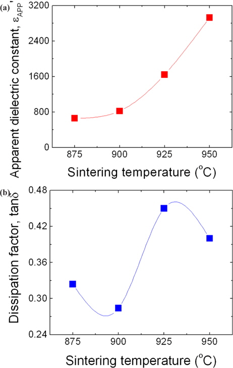
The tendency of change in the εAPP' at 1 kHz as a function of sintering temperature is indicated graphically in Fig. 7(a). εAPP' increased abruptly from 658.6 to 2928.8 in light of the change as small as 75℃ in the total range of the sintering temperature. This is assumed to be a result of the average grain size and depletion layer width, as can be seen in the expression, εAPP' = εg(d/t), where εg is the dielectric constant of ZnO (8.5), d is the average grain size, and t is the depletion layer width of both sides at the grain boundaries. The tendency of change in the tanδ at 1 kHz as a function of sintering temperature is indicated graphically in Fig. 7(b). With the increase of sintering temperature, tanδ decreased from 0.324 to 0.280 until the sintering temperature reached 900℃, and then increased when the sintering temperature was further increased. However, when the sintering temperature exceeded 925℃, it again decreased. As a result, tanδ exhibited a fluctuation because the repletion cycle decreased and increased in the range of sintering temperature. tanδ is composed of the joule loss due to heat generation by leakage current, and frictional loss due to heat generation by electric dipole rotation. The tendency of change of tanδ was very similar to that of leakage current. Therefore, it is assumed that tanδ was strongly affected by the leakage current. The dielectric parameters are summarized in Table 1.
We investigated the tendency of change of the microstructure, electrical properties, and dielectric characteristics of ZnO-V2O5-MnO2-Nb2O5-Dy2O3-based ceramics sintered at different temperatures. Microstructural experiment results showed that the sintered density decreased and the average grain size increased with the increase of sintering temperature. The breakdown field decreased noticeably with the increase of sintering temperature. When the sintering temperature increased, the nonlinear coefficient exhibited a fluctuation and a maximum value of 39.2 at 900℃. Increasing the sintering temperature resulted in an increase in the tendency of change in the dielectric constant and fluctuation behavior in the dissipation factor.