The high efficiency Si solar cell has been extensively investigated to improve the photoreflection (PR) losses, minority carrier generation, recombination loss by surface passivation, and to introduce nanostructures of semiconductor nanoparticles, metal nanoparticles, and nanosurfaces [1-4]. The photoreflectance of the Si solar cells can be further significantly suppressed in the broad spectral range using the nanotexturing process [5-7]. The nanotextured porous silicon provides a graded refractive index between the Si solar cell surface and air that results in a low reflectivity and high photoabsorption of visible light [8]. Therefore, nanotextured Si provides a promising approach to reduce surface reflection to the zeroth order and replace conventional anti-reflection layers in Si solar cells [9,10] that can enhance the conversion efficiency to a greater extent [11].
Several techniques including reactive ion etching (RIE) [2], plasma immersion ion implantation etching [12], metal assisted chemical etching [13] and laser-induced etching [14] have been implemented to form nanotextured Si solar cell surfaces. However, these nanotexturing processes (except for the metal assisted chemical etching process) are rather expensive. Therefore, the metal assisted chemical etching technique has been very popular for the nanotexturing of 6 inch Si solar cell wafers due its low cost and easy preparation technique that significantly reduces the photoreflectance (PR). In the metal assisted chemical etching process, the nanotexturing of Si solar cells can be carried out by directly immersing the cell in a mixed solution of hydrogen fluoride (HF) and AgNO3 for the desired time [15,16]. The fabricated cells with over or non-uniform etching show slight improvement of the conversion efficiency because of their large surface area leading to high surface recombination [15,17]. Therefore, to control the nanotexturing process, it is better to separate the metal assisted chemical etching process as a two-step process (metal pre-deposition and etching process) in order to form a shallow nanotextured surface with low surface and Auger recombination.
In this work, we investigated nanotextured Si solar cells with the metal-assisted chemical etching process using two different concentrations of etching solutions. The one-step etching process with the high concentration of HF:AgNO3 (4:0.2 M) was performed on the microtextured surface of single crystalline Si solar cells in order to form nanowires. The one-step etching process with the low concentration of HF:AgNO3 (0.14:0.005 M) and the further etching process with an etching solution of HF:H2O2:H2O (1:2:10 vol%) were performed. The two-step process showed nano-roughened surface formation with ultra-small nanopores. The high concentration one-step process forms nanowires with excellent optical properties and the low concentration two-step process forms a nano-roughened surface with enhanced electrical properties of the fabricated cells.
Single crystalline p-type boron (B)-doped Si wafers were used for this experimental work. The wafers were 156×156 mm2 in size with a specific resistance of 0.5~3 Ω· cm, and a thickness of 200±5 μm. First, the wafers were dipped in ethanol and placed on a sonicator for 5 min. The same procedure was then followed for cleaning in isopropyl alcohol (IPA) and the wafers were then rinsed in deionized water. After cleaning, the wafers were dried under N2 gas. The wafers were then microtextured by etching in a 10% NaOH solution at 70℃ for 30 min to form micropyramidal structures. This was defined as the fabricated cell of reference (Ref.). A further nanotexturing process was then carried out on the microtextured surface by anodic and cathodic reaction. To form Si nanowires, the microtextured solar cells were dipped in a HF:AgNO3 (4 M:0.2 M) solution at a temperature of 80℃ and then immersed in HNO3 acid to remove the Ag residuals. We defined the samples of the high concentration (HC) one-step process for etching times of 5 min, 1 min, and 30 sec as HC one-step 5 min, HC one-step 1 min, and HC one-step 30 sec, respectively.
The further nanotexturization on the microtextured surface of the solar cells was carried out by reducing the solution concentration in a mixture of HF:AgNO3 (0.14:0.005 M) solution for 5 min and immediately immersing in HNO3 acid for the removal of Ag residuals. The sample with the low concentration (LC) one-step process was defined as a sample of LC one-step 5 min. Furthermore, after dipping in a mixture of HF:AgNO3 (0.14:0.005 M) solution for 5 min, a further two-step process was carried out in an etching solution of HF:H2O2:H2O (1:2:10 vol%) for 30 and 90 sec, the samples of which were defined as LC two-step 30 sec and LC two-step 90 sec, respectively. After the two-step nanotexturization process, the remaining Ag residuals on the solar cell surfaces were removed by concentrated HNO3 acid for 3 min and sufficiently rinsed with DI water. The wafers were then treated by a mixture of HCl:H2SO4:H2O at a volume ratio of 1:1:2 at 70℃ for 10 min in order to remove the HF contaminants remaining after the nanotexturing process. The oxide formed by this process was removed by 10% HF for 1 min.
The emitter layer was formed using a tube furnace diffusion process with POCl3 liquid as the dopant under O2 and N2 as the carrier gases for the pre-deposition and drive-in processes, respectively, to obtain a sheet resistance of 55 Ω/sq. The predeposition process was carried out for 10 min at 750℃, a P2O5 layer formed and worked as a phosphorous dopant source at the Si solar cell surface. The phosphorous dopant was diffused into the solar cell using the drive-in process at 820℃ for 10 min and phosphor-silicate glass (PSG) was formed on the surface. This PSG layer was removed using a 10% HF solution. After the removal of the PSG layer, an 80 nm thick SiNx layer as a surface passivation and anti-reflection coating (ARC) layer was deposited under SiH4:NH3:Ar gas for 10 min using plasma enhanced chemical vapor deposition (PECVD). The front silver pattern contact and aluminum back surface field were formed using a screen-printing technique and were then dried at 200℃. A co-firing process was then carried out in a belt IR furnace at 400~850℃. Finally, the edge isolation process was performed to prevent current leakage.
The samples were characterized by various measurement tools including a field emission scanning electron microscope (FESEM), which was used to study the surface morphology of the cells. The PR of the textured wafers and the fabricated solar cells were measured using a UV-VIS-NIR spectrophotometer. The p-n junction of the solar cells and Ohmic contact properties were characterized from photoluminescence (PL) and electroluminescence (EL) images (McScience Co. K3300). The quantum efficiency (QE) was measured (ICPE system Co. QEX7) with a Xenon arc lamp that converts the incident photons to a current. I-V measurements for cell conversion efficiencies were carried out using a Sun simulation under the conditions of 100 mW/cm2 and AM 1.5 irradiation at 25℃.
A cathodic reaction occurs between the Ag ions and Si, resulting in H2 molecules with the Ag nanoparticles stuck to the Si surface as shown in Fig. 1. In the anodic reaction, Si oxidation occurs by either releasing electrons or consuming holes. The released electrons are transferred to the Ag deposition sites. The transference of electrons causes an electric current (corrosion current) flowing from the local cathode to the anode sites. This causes the deposition of Ag ions in the form of metallic Ag nano-crystallites. Furthermore, the electronegativity of Ag ions here is higher than that of Si. As a result, the Ag nanocrystallites draw the electrons from silicon and become more electronegative. In this way, the Ag nanocrystalites grow into large particles by increasing the etching time. Meanwhile, the Si below the Ag particles releases the same number of electrons as that acquired by the Ag ions, and therefore is reduced by forming a layer of SiO2 at the Ag/Si interface. The SiO2 layer is etched out by the HF solution. During etching, nanopits are formed and Ag nanoparticles enter the nanopits, within which they become trapped. The Ag ions are only allowed to move in the vertical direction of the pits. With the increase in etching time, the nanopits are formed into nanopores and nanowires. As the charge only transfers between the Ag ions and Si particles under the nanopits, no damage occurs to the walls of the nanopits.
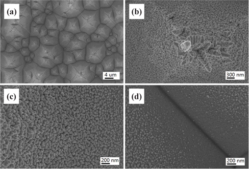
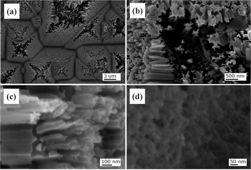
Figure 2 shows FE-SEM images of the nanotextured surfaces for the HC one-step 5 min sample. The micropyramidal structure was totally removed and became a flat surface with the formation of nanopores as shown in Fig. 2(d). The HC etching time of 5 min was too long to retain the micropyramids, and the nanobundles of the nanowires were uniformly formed vertical to the substrate. The deep etching generated pores having sizes of a nanometer scale.
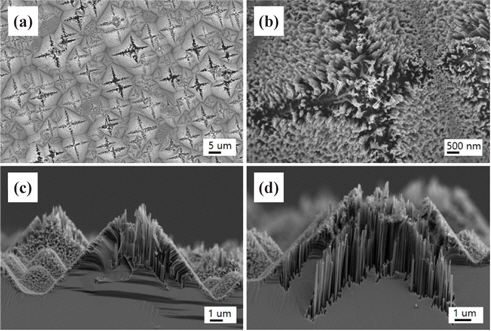
Figure 3 shows FE-SEM images of the nanotextured surfaces for the sample of HC one-step 1 min. The top parts of the pyramids were severely etched out and showed the distinct formation of nanowires, as shown in Fig. 3(b). The hillside and valley areas showed the formation of nanowires as shown in Figs. 3(c) and 3(d).
Figure 4 shows FE-SEM images of the nanotextured surfaces for the HC one-step 30 sec sample. The top parts of the pyramids were also severely etched out and showed the formation of nanowires as shown in Fig. 4(b). In order to understand the nanowire structure, cross-sectional images were measured and showed both [100] and [111] etching directions in the top pyramidal region and hillside region, respectively, as shown in Fig. 4(c). The hillside nanowires were normal to their corresponding (111) planes. The [100] directional nanowires formed of around 3 μm long were mostly interconnected, forming nanopillar structures on the [100] directional wedges as shown in Fig. 4(d). The pyramidal surfaces were etched vertically, showing the formation of pores in the [111] directions with the 400 nm lengthen nanowires. This indicates that the etch rate in the [100] direction is much faster than the rate in the [111] direction.
The continuous oxidation and dissolution of Si in the high concentrated etching solution give rise to the formation of <100>-oriented Si nanowires because of the presence of the two covalent bonds at the Si(100) plane, which favor the etching of Si atoms in the [100] direction [18]. However, the Si atoms in the (111) plane are strongly bonded, which prevents rapid etching of Si in the [111] direction. Therefore, Si nanowires of small nanometer lengths are formed in the <111>-direction. As the latitude of the pyramid is higher, the etching depth is increased, indicating that the pyramid surface is more exposed to the etching solution in the top area. The directional etching in the [111] and [100] directions has been reported by many groups [19,20].
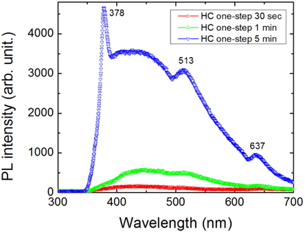
Figure 5 shows the PL spectra for the nanotextured surfaces of samples with an HC one-step process. The PL was measured under 325 nm excitation using a He-Cd laser. All the samples show multiple PL peaks at the wavelengths of 450, 513, and 637 nm (2.75, 2.42, and 1.95 eV). However, the PL intensity of the sample with small nanowires is very low, and is very high for the long nanowire with nanoholes, which indicates that the PL intensity increases when increasing the nanowire length with porosity. The HC one-step 5 min sample shows an additional PL peak at the wavelength of 378 nm (3.27 eV), indicating the nanocavity lasing effect caused by the nanoholes. The nanowires are composed of Si nanocrystals and are interconnected. The increasing PL peak intensity with increasing etching time suggests the presence of nanocrystals due to the quantum confinement effect. For the quantum size effect, however, nanowires with diameters in the range of 35~170 nm could not emit the blue band spectrum of 430 nm [21]. The origin of the luminescence mechanism is attributed to the porous surface and the existence of the localized radiative recombination center is suggested [22,23]. Similarly, When the etching time is decreased, the PL intensity of the samples is decreased, which is consistent with the lower porosity of the sample and contains large sized nanocrystallites. Furthermore, the PL spectra of the Si nanowires associated with the nanocrystals are generally broad and strongly depend on their size distributions. The red color emission at the wavelength of 637 nm originates from the radiative recombination of the surface defect-centers in the Si skeletons with a nanoporous structure. This indicates that the conversion efficiency of the nanoporous Si solar cell is not very high due to the high surface recombination.
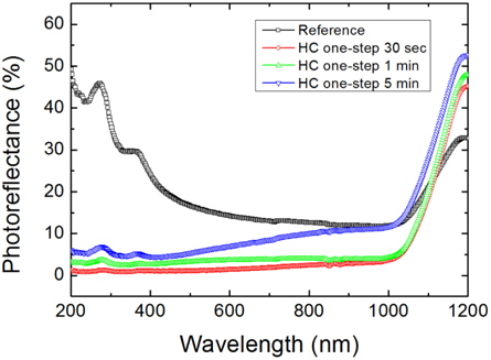
Figure 6 shows the PR spectra of the microtextured Ref. sample and the HC one-step 5 min, 1 min, and 30 sec samples measured using the UV-VIS-IR spectrophotometer. The total PR of the Ref. sample is nearly 20%~30% in the visible spectrum region. However, the HC one-step nanotextured samples for 30 sec, 1 min, and 5 min exhibit a strong decrease of PR below 1%, 3%, and 6%, respectively. As the nanotexturing time increases, the sample shows a transition from nanowires to nanoholes and the PR also tends to increase with an increase in the nanotexturing time, which indicates that Si nanowires are good candidates of light absorption compared to the Si nanoholes. The reduced PR in the UV to IR region of the solar spectrum is similar to black silicon.
The remarkable reduction of the PR in the UV to IR region of the solar spectrum could be due to the three important properties of the Si nanowires: (i) the ultrahigh surface area of the high density nanowires, (ii) the sub-wavelength structured surface of the Si nanowires (which can significantly decrease the PR over a wide spectral bandwidth), and (iii) the Si nanowires with porosity gradient change the refractive index and thus resemble a multi antireflection coating. The ultrahigh surface area of the Si nanowires causes multiple scattering of the incident light between the nanowires to enhance the light trapping. Therefore, superior antireflection characteristics are found for the sample with Si nanowires formed with the etching time of 30 sec. With increasing the etching time, the PR gradually increased due to the decrease in the areal densities of the nanowires. Due to this excellent light absorption property, Si nanowires have also been used for antireflection purposes. The highly surface damaged HC samples show excellent optical properties in light absorption and radiation processes. However, the surface damage is more serious in terms of the electrical property of Si solar cells. We thus further investigated the low surface damaged LC samples for cell fabrication.
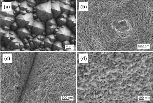
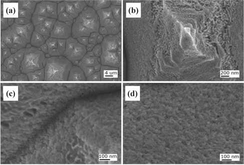
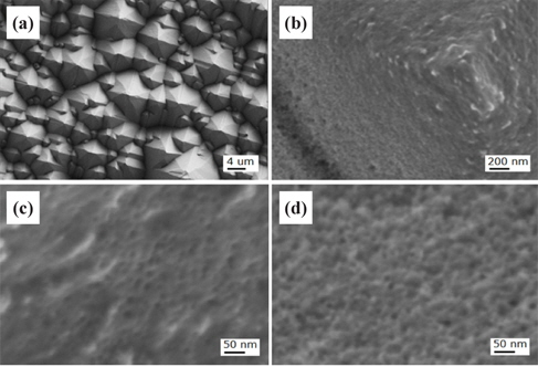
Figure 7 shows the FESEM images of the Si solar cell with the nanotexturing process for the LC one-step 5 min sample. The top of the micropyramid is slightly over-etched, whereby nanoneedles are formed as shown in Fig. 7(b) and a shallow etched surface is clearly seen at the bottom area of the micropyramids in Fig. 7(c).
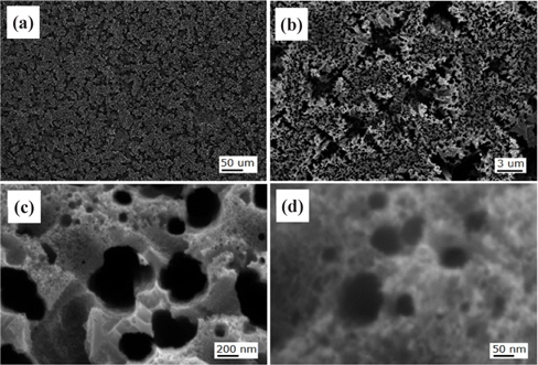
Figure 8 shows the FESEM images of the Si solar cell with the nanotexturing process for the LC two-step 30 sec sample. The cell etched for 30 sec shows ultra-small nanopores with uniform shallow etching on the top and bottom of the microtextured solar cell surface, as shown in Figs. 7(b) and 7(c), respectively. The average diameter of these nanopores is less than 10 nm.
Figure 9 shows the FESEM images of the Si solar cell with nanotexturing process for the LC two-step 90 sec sample. This sample shows that the top and bottom areas are polished and roughened compared to the LC two-step 30 sec sample, indicating that the surface is highly oxidized by H2O2 and dissolved by HF due to the long time taken for etching. Furthermore, for the long time taken for etching, the pore openings become larger and dissolution of the Si walls occurs at the surface. The 30 sec nanotextured solar cells show the best roughness for the nanotextured solar cell fabrication.
In the two-step nanotexturing process in the two-step nanotexturing process, H2O2 plays the role of an oxidizing agent and controls the nanotexturing process in order to form ultra-small Si nanopores and polished Si with low roughness, which is clearly described in previous works [16,24]. However, the one-step nanotexturing process always exhibits large pores perpendicular to the surface [25]. This large surface area from the nanoporous structure is attributed to the poor blue-response and high surface recombination that decreases cell performance. The ultra-small nanopores formed using the two-step nanotexturing process show a very small surface area, which may contribute to improving the cell efficiency due to the high blue response and low surface recombination. Therefore, 6" Si solar cell wafers textured using the two-step nanotexturing process were used to fabricate Si solar cells and were compared with the fabricated one-step nanotextured and reference solar cells.
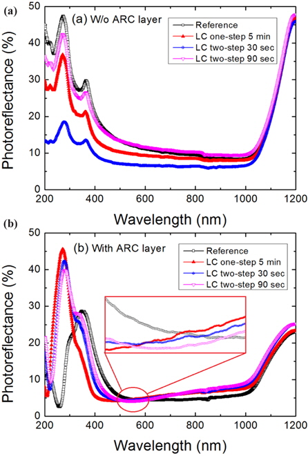
Figure 10 shows the PR spectra of the Ref. and nanotextured samples without (a) and with (b) the ARC layer in the wavelength range of 200~1,200 nm. The PR spectra of the samples were measured using a UV-VIS-IR spectrophotometer (UV-3600, Shimadzu Co. Japan). In Fig. 10(a), the sample nanotextured for 90 sec shows slightly reduced PR in the UV/VIS spectral region of the wavelength range of 200~500 nm compared to the Ref. sample, but the PR increases in the VIS/IR region. The PR of the sample nanotextured for 5 min using the one-step process is reduced in all spectral regions compared to the Ref. and the 90 sec nanotextured sample. The sample nanotextured for 30 sec shows the lowest PR from the UV to IR region of the solar spectrum, indicating excellent surface roughness. Similarly, the PR of the nanotextured fabricated cells with the ARC layer, shown in Fig. 10(b), is found to be significantly reduced to less than 5% in the wavelength range of 347~600 nm and 10% in the wavelength range of 600~1,100 nm. However, the PR of the nanotextured cells in the wavelength range of 600~1,100 nm is higher than that of the Ref. cell. Furthermore, the one-step 5 min nanotextured cell shows the lowest PR in the wavelength range of 337~564 nm, while the two-step 30 and 90 sec nanotextured cells show reduced PR in the wavelength range of 337~582 nm and 337~600 nm, respectively, compared to the Ref. cell. However, the PR of the two-step nanotextured cells was significantly reduced in the green and red regions of the wavelength range of 521~700 nm compared to the one-step 5 min nanotextured cell. This indicates that ultra-nanopores are effective for absorbing light in the green and red spectral region.
The nanotextured silicon consists of Si nanocrystals and nanopores which reduces the refractive index. Therefore, the sample nanotextured for 30 sec by two-step process reduced the refractive index and PR in all wavelengths of the solar spectrum with respect to the increase of nanopore densities [26]. The PR of the cells in the wavelength range of 600~1,100 nm with ARC layer increased due to the random distribution of nanopores and increased roughness of the nanoporous Si surface. The increased light absorption in the wavelength range from 347 to 600 nm indicates the widening band gap of the porous silicon layer due to the quantum confinement effect of the porous Si nanocrystals which can enhance the conversion efficiency of the nanotextured Si solar cells [27]. The improved light absorption the improved light absorption of the two-step nanotextured cells in the green and red spectral region indicates that the two-step nanotextured cells exhibit superior photo absorption property and may contribute to improving the conversion efficiency more than the one-step nanotextured cell. The one-step nanotextured cell the one-step nanotextured cell has low PR in the short wavelength region compared to the two-step nanotextured cells, indicating the necessity of nanostructures with large surface area. However, there are many possibilities of surface recombination by the dangling bonds of the nanostructures with large surface area that reduce the short-circuit current [28].
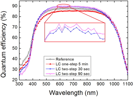
Figure 11 shows the quantum efficiency of the Ref. and the nanotextured cells etched for 5 min using the one-step process for 30 sec, and the two-step process for 90 sec. The quantum efficiency of the Ref., and the cells nanotextured for one-step 5 min and two-step 30 sec are 87.85%, 85.57%, and 89.77% at the wavelengths of 670, 730, and 630 nm, respectively. However, the quantum efficiency of the cell nanotextured for 90 sec using the two-step process is 89.95% at the wavelength of 610 nm. The cells nanotextured using the two-step process show an enhancement in quantum efficiency of around 2% and 4% compared to the Ref. and one-step nanotextured cells, respectively. Furthermore, the two-step 30 and two-step 60 sec nanotextured cells demonstrate higher quantum efficiencies in the visible-IR wavelength ranges of 434~900 nm and 464~1,000 nm, respectively, than the reference cell. However, the cell nanotextured for 5 min using the one-step process has the lowest quantum efficiency. The improved quantum efficiency of the two-step nanotextured cells is consistent with the reversed PR in the wavelength range of 400~600 nm but is inconsistent in the IR region of the solar spectrum.
The two-step nanotextured cells show improved blue light response at shorter wavelengths of 434 and 464 nm for etching times 30 and 90 sec, respectively. The ultra-small nanopores are effective in maintaining the surface passivation properties and improving the collection ability of the photon generated carriers with reduced surface recombination [29,30]. However, the cell nanotextured for 5 min using one-step process shows reduced blue response in the quantum efficiency, which may be due to the increased surface area that increases the surface recombination.
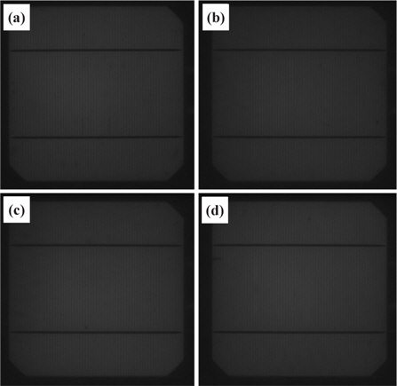
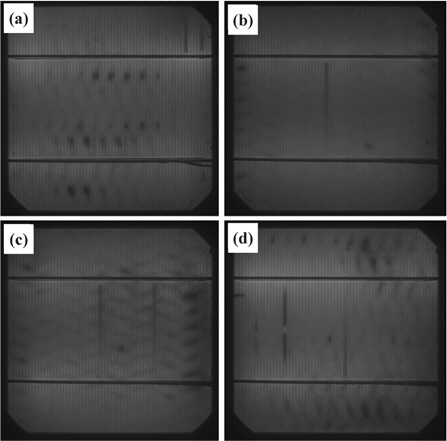
Figure 12 shows the photographic photoluminescence (PL) images of the reference (a), the cell nanotextured for 5 min with the one-step process (b), 30 sec (c), and 90 sec (d) with the twostep process. The cells nanotextured for 30 and 90 sec using the two-step nanotexturing process are slightly brighter than the Ref. and 5 min nanotextured cell, which indicates that the formation of the pn junction is not disturbed by the ultra-small nanopores formed by the two-step nanotexturing process. Similarly, the photographic electroluminescence (EL) images of the reference and nanotextured cells are shown in Fig. 13. Figure 13(a) shows the EL image of the reference cell and 13(b), 13(c), and 13(d) show the EL images of the cells nanotextured for 5 min, 30 sec, and 90 sec, respectively. In the EL images, the 90 sec nanotextured cell is brighter under the finger and bus bars than the other nanotextured and reference cells. However, the 30 sec nanotextured cell is relatively brighter in all parts. The bright EL images of the cells nanotextured with the two-step process indicate that Ohmic contact resistance can be more significantly reduced by the ultra-small nanopores compared to the cell with large surface area nanopores formed with the one-step nanotexturing process. Therefore, ultra-small nanopores are efficient in current movement from the electrode to the pn junction. Some broken fingerlines and dark spots can be clearly seen in each cell, which causes electron loss and shunt resistance problems, respectively.
Since nanopores with a large surface area lead to surface recombination due to the oxygen related dangling bond density [31], the luminescence emissivity of the 5 min nanotextured cell is more reduced than the cells with ultra-small nanopores formed using the two-step nanotexturing process. Therefore, the ultra-small nanopores with low pore depth and density are excellent in reducing surface recombination that increases the luminescence emissivity. The dark spot in both the PL and EL images of the nanotextured cells indicates the formation of damage during the cell fabrication process which can degrade the cell performance due to the current leakage across the junction. The EL and PL images show the superiority of the two-step nanotextured cells over the one-step nanotextured cell, indicating that low dimensional nanostructures can reduce the surface recombination probability that results in the enhancement of cell performance [32].
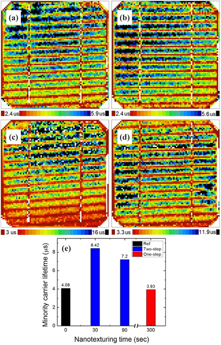
Figure 14 shows the high resolution minority carrier lifetime mapping of the hydrogen implanted Si solar cells. The measurement was performed with a SEMILAB WT2000 microwave photoconductive decay (μ-PCD) system with the excitation light of a 904 nm laser diode. In the images, the red zones show the minimum and black zones show the maximum lifetime of the minority carriers. The minority carrier lifetime image of the reference cell is shown in Fig. 14(a) and the cells nanotextured for 5 min, 30 sec, and 90 sec by one-step and two-step nanotexturing processes are shown in Figs. 14(b), 14(c), and 14(d), respectively. The average minority carrier lifetimes of the reference and the nanotextured cells are shown in Fig. 14(e). The average minority carrier lifetimes of the Ref., one-step 5 min, two-step 30 sec, and two-step 90 sec nanotextured cells are 4.08, 3.93, 8.42, and 7.2 μs, respectively. The above results reveal that ultra-small nanopores formed from the two-step nanotexturing process for a nanotexturing time of 30 sec are effective in surface passivation that reduces the surface recombination. However, the minority carrier lifetime of the cell nanotextured for 5 min using the onestep nanotexturing process is lower than the Ref. and two-step process nanotextured cells, which indicates that nanopores with high surface area increase the dangling bond related surface defects that increase the surface recombination.
Since the nanopores formed using the one-step nanotexturing process have a large surface area that induces dangling bonds, the surface cannot be effectively passivated by SiNx to saturate these dangling bonds. Hence, the poor passivation of these nanostructures contributes to increase the surface recombination as well as the Auger recombination [33]. The dangling bonds can be minimized by reducing the surface area, which occurred with the two-step nanotexturing process. Therefore, the cell with ultra-small nanopores formed by the two-step nanotexturing process demonstrates a high minority carrier lifetime because of the low surface recombination of the due to the small surface area [34]. Furthermore, to compare the well-rounded curvature or microtextured surface with the, wedge-type nanoporous structure or nanotextured surface shows the enhanced overdoping to form dead-layer during doping process [35]. The one-step nanotexturing process forms a dead-layer which causes high Auger recombination. However, our result of minority carrier lifetime enhancement illustrates that the ultra-small nanopores formed from the two-step nanotexturing process can effectively reduce the dead layer and the nanosurface curvature is reduced, which suppresses both the surface and Auger recombination.
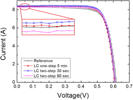
Figure 15 shows the I-V characteristics of the fabricated reference and nanotextured cells measured using a solar simulator under the conditions of 100 mW/cm2 and AM 1.5 irradiation at 25℃ and the data have been summarized in Table 1. The cell nanotextured for 30 sec using a two-step nanotexturing process shows the highest conversion efficiency of 16.9%, with short circuit current (Isc) = 8.377 A, open circuit voltage (Voc) = 0.610 V, fill factor (FF) = 78.87%, series resistance (Rs) = 0.007 Ω, and shunt resistance (Rsh) = 9.98 Ω. The reference cell shows the efficiency of 16.3% with Isc = 8.338 A, Voc = 0.618 V, FF = 75.69%, Rs = 0.008 Ω, and Rsh = 4.504 Ω. Similarly, the performance of the one-step nanotextured cell etched for 5 min has the conversion efficiency of 16.7% with Isc = 8.346 A, Voc = 0.607 V, FF = 78.27%, Rs = 0.007 Ω, and Rsh = 32.82 Ω. The cell nanotextured for 90 sec with the two-step nanotexturing process has the conversion efficiency of 16.7%, with Isc = 8.278 A, Voc = 0.612 V, FF = 78.83%, Rs = 0.008 Ω, and Rsh = 9.84 Ω.
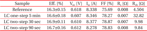
Performance of the fabricated Si solar cells with low concentration one- and two-step nanotexturing processes.
The conversion efficiency of the two-step nanotextured cells is consistent with PR, QE, EL, PL, and minority carrier lifetime. However, the efficiency of the one-step nanotextured cell is not consistent with the QE, EL, PL, and minority carrier lifetime. The conversion efficiency of the one-step nanotextured cell is 0.3% higher than that of the Ref. cell, which may be due to the enhanced photoabsorption in the UV-VIS spectral region. Furthermore, the improved FF and Rsh of the one-step nanotextured cell indicate that the p-n junction is not significantly affected by the nanotexturing process. Since the Rsh is correlated with the dark spots, so the number of dark spots in the two-step nanotextured cells is more than the one-step nanotextured cell, which gives rise to a low Rsh. The nanotextured cell for 30 sec with the two-step nanotexturing process has higher efficiencies of 0.6% and 0.3% than the reference and one-step nanotextured cells, respectively, due to higher Isc as a result of the excellent blue-response of the ultra-small nanopores and improved minority carrier lifetime. The reduced surface recombination by the two-step nanotexturing process can also reduce the dark saturation current (Io) of solar cells [36], which can further increase the Voc according to the Eq. (1) in Ref [37]

where kB is the Boltzmann’s constant, T is the temperature, q is the charge of an electron, and Isc is the short-circuit current. The nanotextured cells show slightly lower values of Voc than those of the Ref. cell. This is probably due to the poor passivation of the SiNx layer for the nanotextured surface [38]. Therefore, a better passivation is still required for the nanotextured Si solar cell that can improve both Isc and Voc by effectively suppressing the surface and Auger recombination.
We performed high and low concentration nanotexturing processes of Ag metal-assisted chemical etching. The high concentration nanotexturing process showed severe surface damage with nanowire formation on the top regions of micropyramids and remarkable photoreflectance reduction with strong photoluminescence. The low concentration nanotexturing process showed nano-roughened surfaces with slight enhancement of photoreflectance. The fabrication of 6-inch microtextured Si solar cells was carried out with a low concentration nanotexturing process. The results of the reference and low concentration one-step nanotextured cells were compared to results from the wafer with two-step nanotexturing process by adding a mixed chemical solution of HF:H2O2:H2O (1:2:10 vol%) for 30 and 90 sec. Ultra-small nanopores were observed on the surface of the 30 sec-nanotextured solar cells and when the etching time was increased to 90 sec, the nanopores were dissolved and changed to polished surfaces with a narrow nanopore density. The PR of the two-step nanotextured cells was found to be decreased in the wavelength range of 337~600 nm, which is better than that of the one-step and reference solar cell. The improved minority carrier lifetime of the solar cell with these ultra-small nanopores suggests better surface passivation of the SiNx, reducing the surface and Auger recombination and hence improving the conversion efficiency by up to 16.9%. In conclusion, the surface nanowire in the high concentration nanotexturing sample is effective for the optical properties, while the nano-roughened surface in the low concentration two-step process is effective for the electrical properties by reducing the formation of the over-doped dead layer.