In recent years, graphene, a 2D hexagonal structure of sp2 bonded carbon atoms [1] that are one atomic layer thick (~0.315 nm) [2]. Graphene has attracted significant attention from optoelectronics engineers and researchers in healthcare and medical engineering fields, because of its unique electrical, chemical, optical and mechanical properties and outstanding details in terms of its electronics band structure [1-4]. These remarkable properties of graphene offer an excellent material for a large number of different nanoelectronic and photonic applications, such as high speed transistors [5], biomechanical sensors [6], high frequency photodetectors [7] and saturable absorbers [8]. Although high quality graphene films can be grown using epitaxial synthesis and chemical vapor deposition (CVD) [9-13], the fabrication of specific structures, such as graphene ribbons, graphene pads or graphene electrodes, still remain a challenge due to the engineering challenge of controlling the number of graphene layers in a multi-layered graphene film. The graphene based nanodecive performance can be significantly altered by the presence of fabrication residue [14]. Hence, the fabrication of the high quality and high uniformity of nanoscale structures using single/bi-layer graphene is still a major challenge in advanced nanofabrication.
There are many ways to pattern nanostructures on graphene films. These ways include plasma etching [15], reactive ion etching [3], gas phase etching process [16], atomic layer etching [17] and electron beam photolithography [18,19].
Oxygen plasma cleaning etch was usually used to remove the etching residue or graphene layers without controlling the number of layers that were being removed. Recently, Fabo et al. [3] used the oxygen plasma etching to remove one layer of graphene using poly(methyl methacrylate) (PMMA) as protecting layer. Single-layer graphene from bi-layer graphene sheets was achieved successfully through 17 s of etching the bi-layer graphene sample in an RIE system. The gas flow rate, radio frequency (RF) power, and working pressure of the chamber were 10 sccm, 70 W and 313~317 mTorr respectively. Although a monolayer graphene was achieved from the bi-layer graphene flakes, using long processing time could produce several defects on the graphene sheets, such as the reverse deposition of a carbon compound on the graphene sheet. This occurs through epoxy and carbonyl covalent bonds in the sp2 hybridization [20].
Prado et.al [14] employed the RIE process and plasma cleaning to remove the monolayer of graphene. Based on their observation the graphene layers can be etched using O2 or Ar as etchant gas. The optimum etching time of monolayer graphene was 15 s and 8 min, respectively, by using RIE and plasma techniques and Ar as etchant gas. By using the O2 as the etchant gas, the optimum etching time was reported as 15 s and 3 min respectively for RIE and plasma techniques.
Although several studies have researched graphene layer engineering using different etching technique and different etchant gases, there has not been any research report that has comprehensively studied the effects of using different types of RIE etching masks on the quality of engineered graphene layers.
In this research, we compare the effects of using polystyrene (PS) and conventional photolithography resist (AZ 300) as protective materials on the number of layers engineered from the uniform graphene film using the RIE method.
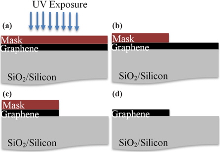
A series of bi-layer graphene films (grown on SiO2/Si substrate using CVD method, from ACS MATERIALS.) were coated with 200 nm of conventional positive AZ 300 photo-resist (PR) and 70 nm of polystyrene. The polystyrene solution was prepared by dispersing 2 wt% polystyrene (PS) latex particles (from Alfa Aesar) in 25 ml of toluene. The etching mask was (i.e. PS or PR) deposited on the graphene film surface by means of a spin-casted method at a speed of 2,000 rpm for 40 s followed by three minutes of soft-baking at 120℃. The PR and PS films were patterned using contact mask-aligner (SUSS-MA6) as shown in Fig. 1(a) and Fig. 1(b). After an appropriate exposure time (i.e. 6 s) and exposure power of 1 mW/cm2 (λ=360 nm), the developing process was carried out using MF319 and MIBK: IPA, 3:1, developer for 5 s and 10 s, respectively, for samples with PR and PS masks. In the next step, samples were post baked to increase the adhesion and resilience of the protective materials to erosion during the RIE process as schematically depicted in Fig. (1).
The RIE experiments were carried out at a different etching time in the range of 3 s to 9 s using a commercial Phantom II Reactive Ion Etching system (Trion Technology Inc.). The processing parameters were fixed as: O2 (etchant gas) with a flow rate of 10 sccm (standard cubic centimeters per minute unit), a working pressure of 200 mTorr and an RF power density of 0.015 W/cm2 for both graphene films that were covered by conventional PR and PS polymers. The etching process parameters, such as etchant gas flow rate, RF power density and working pressure were optimized after a series of experiments based on the reported parameters in the literature [3,9,14].
Raman spectroscopy is a powerful technique in characterizing the quality of the graphene films and investigating the number of layers [21,22] in engineered graphene based devices. This technique is the more common and accurate characterization method in comparison to other techniques, such as atomic force microscopy (AFM) and optical microscopy. In a recorded Raman spectrum of graphene samples, the I2D/IG ratio is strongly correlated to the number of layers in the graphene sample [23]. In a monolayer graphene, this ratio is I2D/IG >2, while for bi-layer graphene film the ratio is 1
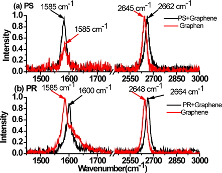
The recorded Raman spectra of both graphene and the protected surfaces before the RIE process are shown in Fig. (2). The I2D/IG ratio and the full width at half maximum (FWHM) of the 2D band were calculated and compared in Table 1. From this table, it is clear that both covered and uncovered surfaces offer bi-layer graphene with a broad 2D band with FWHM in the range of between 27.65 and 34.50 cm−1. The effects of the chemical reaction and different molecular bond formations between the carbon atoms in the graphene structure and the PS were observed as a blue shift in the recorded Raman spectrum of the 2D band and seen to increase in the FWHM value as it is evident from Fig. 2(a). The calculated I2D/IG ratio and FWHM of 2D band values were reduced from 1.90 to 1.07 and from 34 cm−1 to 30.64 cm−1, respectively, as result of PS deposition of 70 nm on the graphene surface. Depositing 200 nm of PR on the graphene surface resulted in a red shift in the peak position and broadening of the G band as indicated in Fig. 2(b). Small differences between the I2D/IG ratio of the two surfaces were recorded by covering the graphene surface with AZ300 as detailed in Table 1. The FWHM reduced from 32.83 cm−1 to 31.05 cm−1 by covering the graphene surface with PR; this is summarized in Table 1. These reductions in the I2D/IG and the FWHM of the 2D band confirm more production of sp3 chemical bonds between the AZ300 polymeric chains and graphene surface.
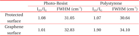
The I2D/IG and FWHM values of both protected and unprotected surfaces before the RIE process. The excitation wavelength and laser power were fixed at 632.8 nm and 20 mW, respectively.
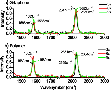
Figure 3 shows the Raman spectrum of both unprotected and protected surfaces of graphene films covered by 70 nm of PS after different RIE processing times in the range of 3 s to 9 s. As shown in Fig. 3(a) and detailed in Table 2, after 9 s of RIE the Raman spectroscopy still proposed a bilayer graphene. From this table it is evident that the I2D/IG ratio of the protected surface was varied between 1.22 and 1.52 during the RIE process, which is close to the ratios before the RIE process (Table 1). After 3 s of RIE, a single layer graphene film was achieved (I2D/IG=2.12) from the bi-layer graphene film. Increasing the RIE processing time to 6 s also offers a single layer graphene with higher G and D band intensity. Applying 9 s of RIE reduces the I2D/IG ratio from 2.02 to 1.54.
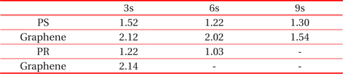
The I2D/IG ratio of both unprotected and protected graphene surfaces after different RIE processing times in the range of 3 s to 9 s. The excitation wavelength and laser power were fixed at 632.8 nm and 20 mW, respectively.
As reported in Table 2, the calculated I2D/IG ratio of the graphene surface in the protected sample with PS was reduced from 2.02 to 1.54 after 9 s of the RIE process. This reduction in the calculated I2D/IG ratio could be attributed to the post-deposition of the etching residue from the mask on the graphene surface and protecting the surface from further etching through the molecular reaction between the carbon atoms in the graphene and the PS films. Hence, the calculated I2D/IG ratio was smaller after 9 s of etching than after 6 s of etching
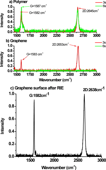
The Raman spectrum of both graphene and covered graphene surfaces with 200 nm of PR are compared in Fig. 4(a) and Fig. 4(b). As indicated in Fig. 4(a), no significant changes were recorded in the position of the G and 2D bands in the covered surface after 6 s of RIE. The I2D/IG ratio was calculated as 1.22 and 1.03 after 3 s and 6 s of RIE, respectively. These results are similar to the calculated ratio before the RIE process (i.e. I2D/IG=1.08).
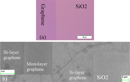
Figure 4(b) shows the Raman spectrum of the graphene surface before etching, after 3 s and after 6 s of RIE. The 2D and G bands were recorded at 2653 cm−1 and 1583 cm−1, respectively, and the I2D/IG was calculated as 2.14. In this figure, it is evident that after 6 s of RIE, the graphene was completely etched and there were no signs of the G and 2D bands in the recorded Raman spectrum. Figure 4(c) shows the recorded Raman spectrum of the graphene surfaces after removing the etching mask (PR). The I2D/ IG ratio was calculated as 1.10. As shown in Fig. 4(c), no significant changes in the Raman spectrum of the graphene surface were recorded after the RIE process and the removal of the PR mask. Figure 5(a) and 5(b) show optical and SEM images of etched bi-layer graphene samples after 6 s. The inset SEM image shows the monolayer graphene etched film after 3 s of the RIE process. As shown in Fig. 5(b), there was no etching residue after 6 s of the RIE process on the bi-layer graphene film on using the PR etching mask.
As can be concluded from Table 2 and Figs. 4(c) and 5, the reaction between the PR etching residue and the graphene surface after 6 s of RIE is less than the reaction when using PS as an etching mask.
This research studied the effects of using two different etching masks, photo-resist and polystyrene on the engineering of graphene layers. The study found that the photo-resist mask is more resistant than the polystyrene masks during the etching process and it produces lower post effects, such as post deposition of etching residue on the graphene surface. Achieving single layer graphene was confirmed by Raman spectroscopy after 6 s of the RIE process and using the oxygen at a flow rate of 10 sccm, RF power density of 0.0015 W/cm2 and working pressure of 200 mTorr. In this study, the achieved etching time for a single layer graphene film grown by CVD was significantly smaller than reported values (15 s) for a graphene flake [14].